Reduced area active above-ground and below-supply noise suppression circuits

Inactive Publication Date: 2009-03-31
IBM CORP
View PDF6 Cites 5 Cited by
  • Summary
  • Abstract
  • Description
  • Claims
  • Application Information

AI Technical Summary

Benefits of technology

[0009]The illustrative embodiments provide a method and apparatus for noise suppression. A circuit has a noise detection unit, a noise suppression unit, and a control unit. The noise suppression unit has an input and an output, wherein the input of the noise detection unit is connected to a signal and generates a signal change at the output if a change in the signal is detected. The noise suppression unit has an input and an

Problems solved by technology

As engineers seek ever increasing speeds in very large scale integration (VLSI) chips, complex problems continue to rise to the forefront.
For example, as process feature sizes continue to shrink, metallurgical limitations are continually raising line-to-line interconnect coupling effects.
Of these directions, two may cause errors in circuit operations.
Above-ground and below-supply signal noise can cause false switching events if the coupling effects causes the voltage level of a signal to cross the switching threshold of a given destination circuit.
Below-ground signal noise and above-supply signal noise can cause a loss of state in certain types of large circuits.
These circuits, however, require a significant area on the chip to include this type of circuit.
This increased use in area can be difficult in applications in which adding circuitry is costly or prohibited.

Method used


Image

  • Reduced area active above-ground and below-supply noise suppression circuits
  • Reduced area active above-ground and below-supply noise suppression circuits
  • Reduced area active above-ground and below-supply noise suppression circuits

Examples


Embodiment Construction

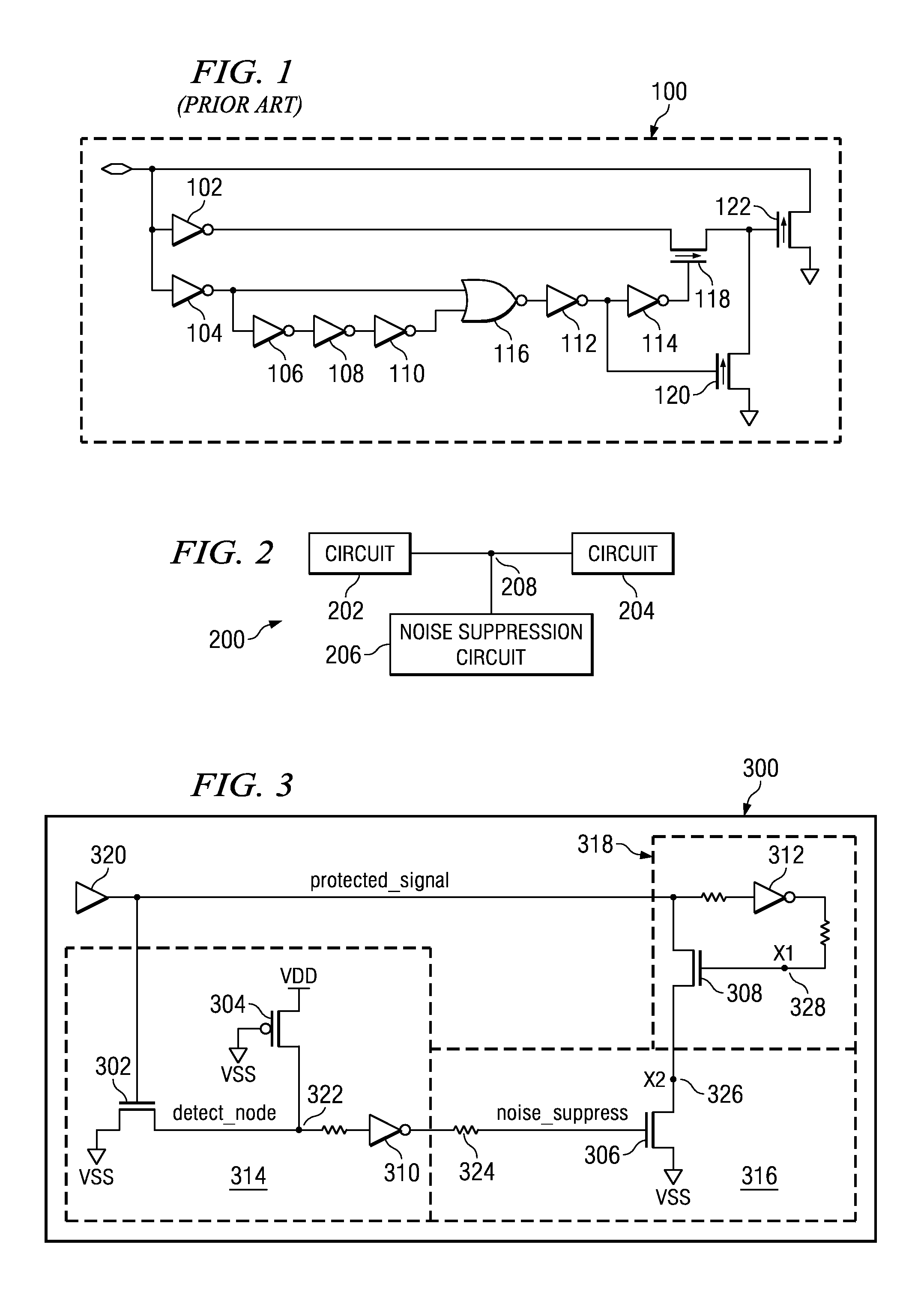
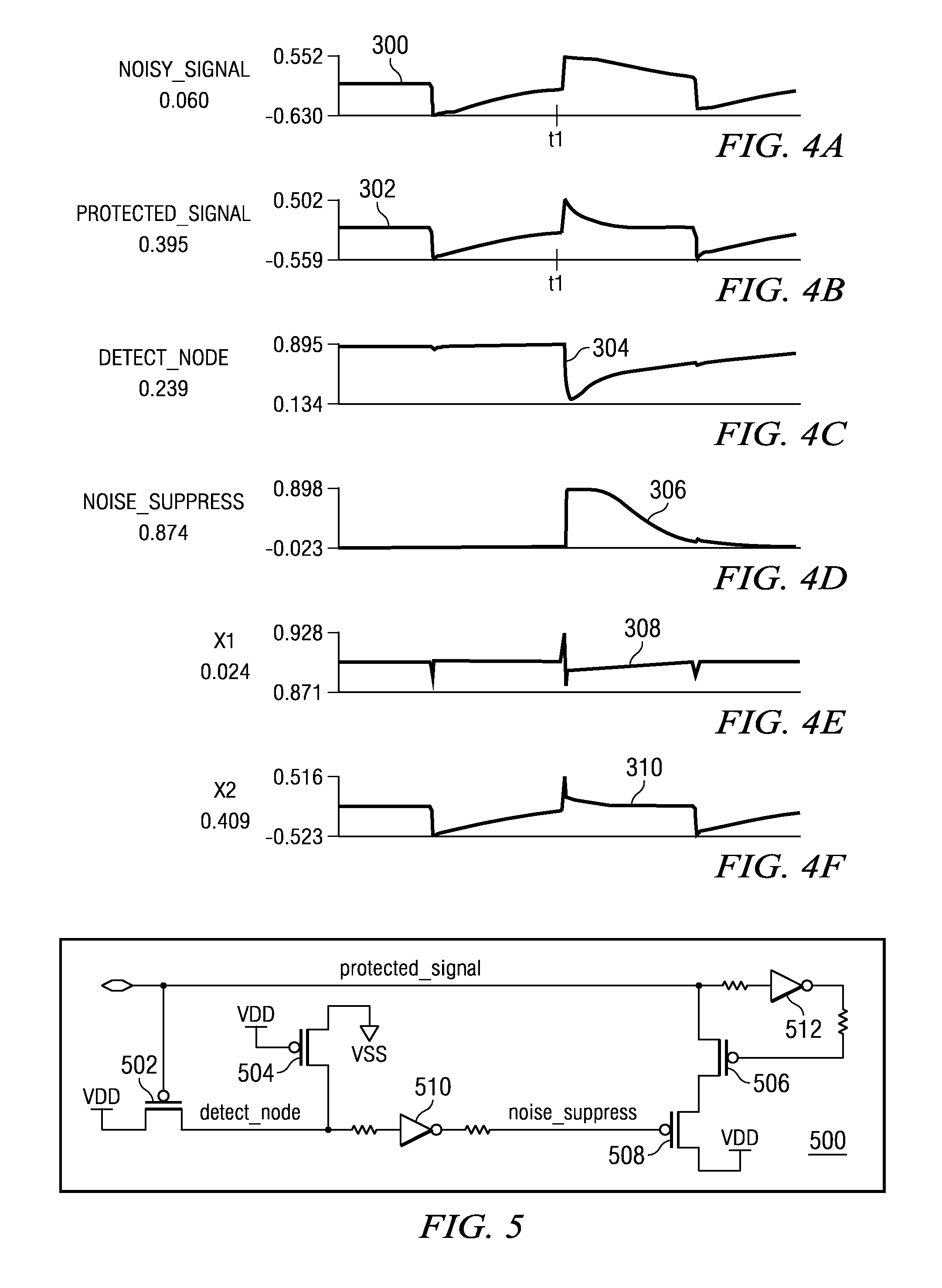
[0016]With reference now to the figures and particularly with reference to FIG. 1, a diagram of a currently used above-ground noise cancellation circuit is depicted. Noise suppression circuit 100 contains inverters 102, 104, 106, 108, 110, 112, 114. Additionally, this circuit also contains NAND gate 116 along with transistors 118, 120, and 122. Each of the inverters in noise suppression circuit 100 requires two transistors to implement. NAND gate 116 includes three transistors. As a result, noise suppression circuit 100, in this example, requires twenty-one transistors to implement.

[0017]Adding twenty-one transistors to a chip requires additional area on the chip for noise suppression circuit 100. In some cases, this additional area may be considered significant, costly, or even prohibited.

[0018]Turning now to FIG. 2, a diagram illustrating a circuit system is depicted in accordance with an advantageous embodiment of the present invention. In this example, circuit system 200 contain...


PUM


Abstract

A method and apparatus for noise suppression. A circuit has a noise detection unit, a noise suppression unit, and a control unit. The noise suppression unit has an input and an output, wherein the input of the noise detection unit is connected to a signal and generates a signal change at the output if a change in the signal is detected. The noise suppression unit has an input and an output, wherein the input of the noise suppression unit is connected to the output of the noise detection unit and generates a correction to the signal in response to detecting the signal change at the output of the noise detection unit. The control unit has an input and an output, wherein input to the control unit is connected to the signal and turns off the noise suppression unit if a state change is detected in the signal.

Description

BACKGROUND OF THE INVENTION[0001]1. Field of the Invention[0002]The present invention relates to electronic circuits and in particular to electric noise suppression circuits.[0003]2. Description of the Related Art[0004]As engineers seek ever increasing speeds in very large scale integration (VLSI) chips, complex problems continue to rise to the forefront. For example, as process feature sizes continue to shrink, metallurgical limitations are continually raising line-to-line interconnect coupling effects. These effects lead to increased concern over signal noise and noise tolerance. Design engineers continually fight and solve problems relating to signal noise.[0005]Signal noise can take several forms. Due to coupling effects, signals can bounce in one or more of four distinct directions: above the ground, below the supply, below the ground, and above the supply. Of these directions, two may cause errors in circuit operations. Above-ground and below-supply signal noise can cause fals...

Claims


Application Information

Patent Timeline
IPC IPC(8): H03K19/003
CPCH03K19/00361
Inventor DAGHER, RAFIKDURHAM, CHRISTOPHER M.KLIM, PETER J.
Owner IBM CORP
Why Eureka
Try Eureka