Apparatus and method for dynamic in-circuit probing of field programmable gate arrays

a gate array and in-circuit probing technology, applied in power supply testing, instruments, measurement devices, etc., can solve the problems of limited power, input and output pins of fpgas, and limited external visibility of most of the signals to electronic test and measurement equipment, and achieve the effect of reducing the external visibility of most signals

Inactive Publication Date: 2009-04-14
KEYSIGHT TECH
View PDF11 Cites 18 Cited by
  • Summary
  • Abstract
  • Description
  • Claims
  • Application Information

AI Technical Summary

Problems solved by technology

However the reality is that this is usually not the case and most designs require extensive in-circuit testing.
From a testing perspective, most FPGAs have a limited number of power, input, and output pins, especially when compared to the amount of signals that exist within an FPGA.
This limits the external visibility of most of the signals to electronic test and measurement equipment.
As a result, debugging a design can become a painstaking, time-consuming, and error-prone process.
Additionally, each design compilation has the potential of subtly altering the timing characteristics of the FPGA because of changes in signal routing and capacitive loading.
The mere process of recompiling the FPGA, even with seemingly minor changes, has the potential to inject non-deterministic timing issues that could cause the design to operate incorrectly, thus requiring further design changes and recompilation.

Method used


Image

  • Apparatus and method for dynamic in-circuit probing of field programmable gate arrays
  • Apparatus and method for dynamic in-circuit probing of field programmable gate arrays
  • Apparatus and method for dynamic in-circuit probing of field programmable gate arrays

Examples


Embodiment Construction

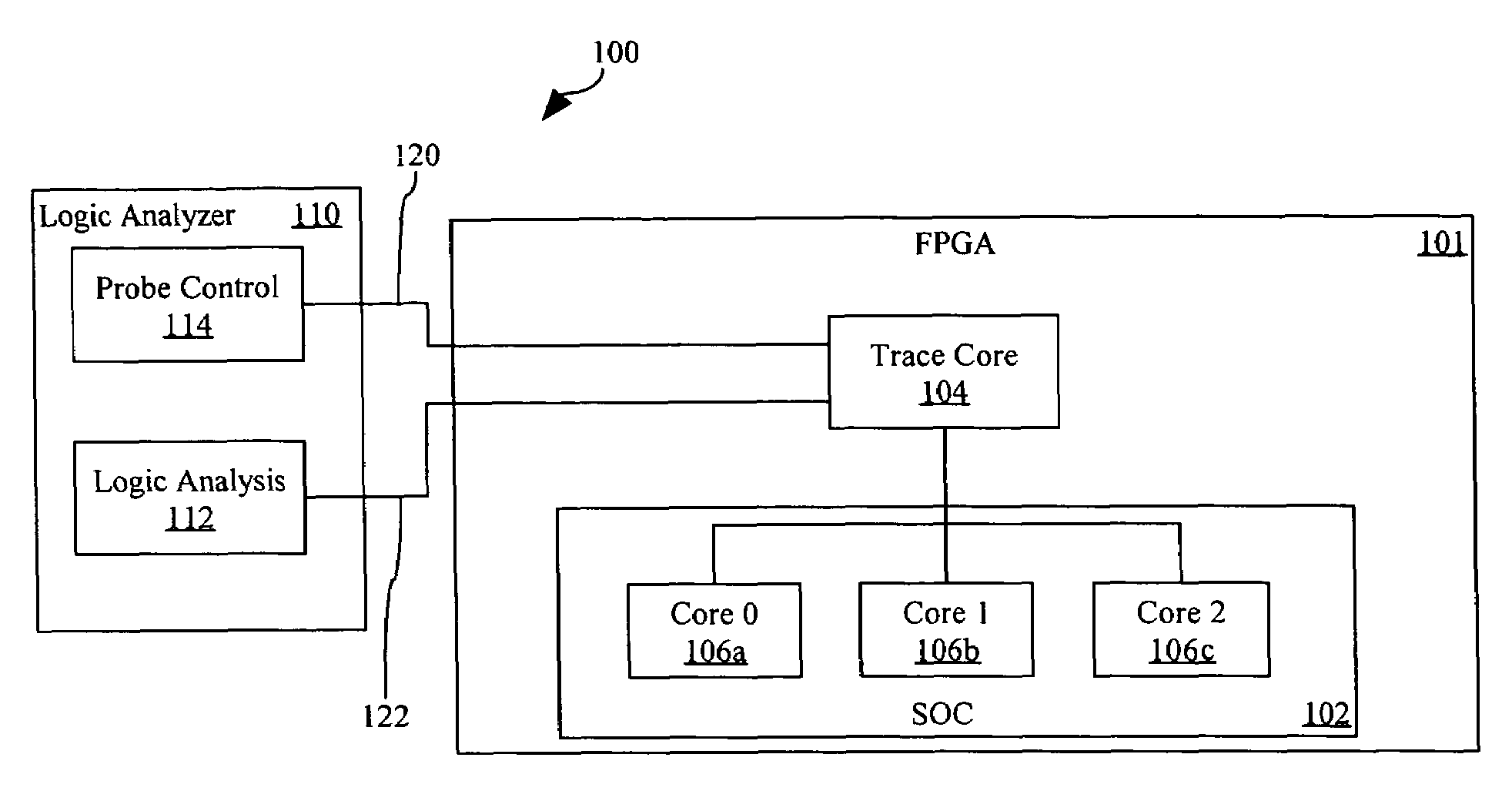
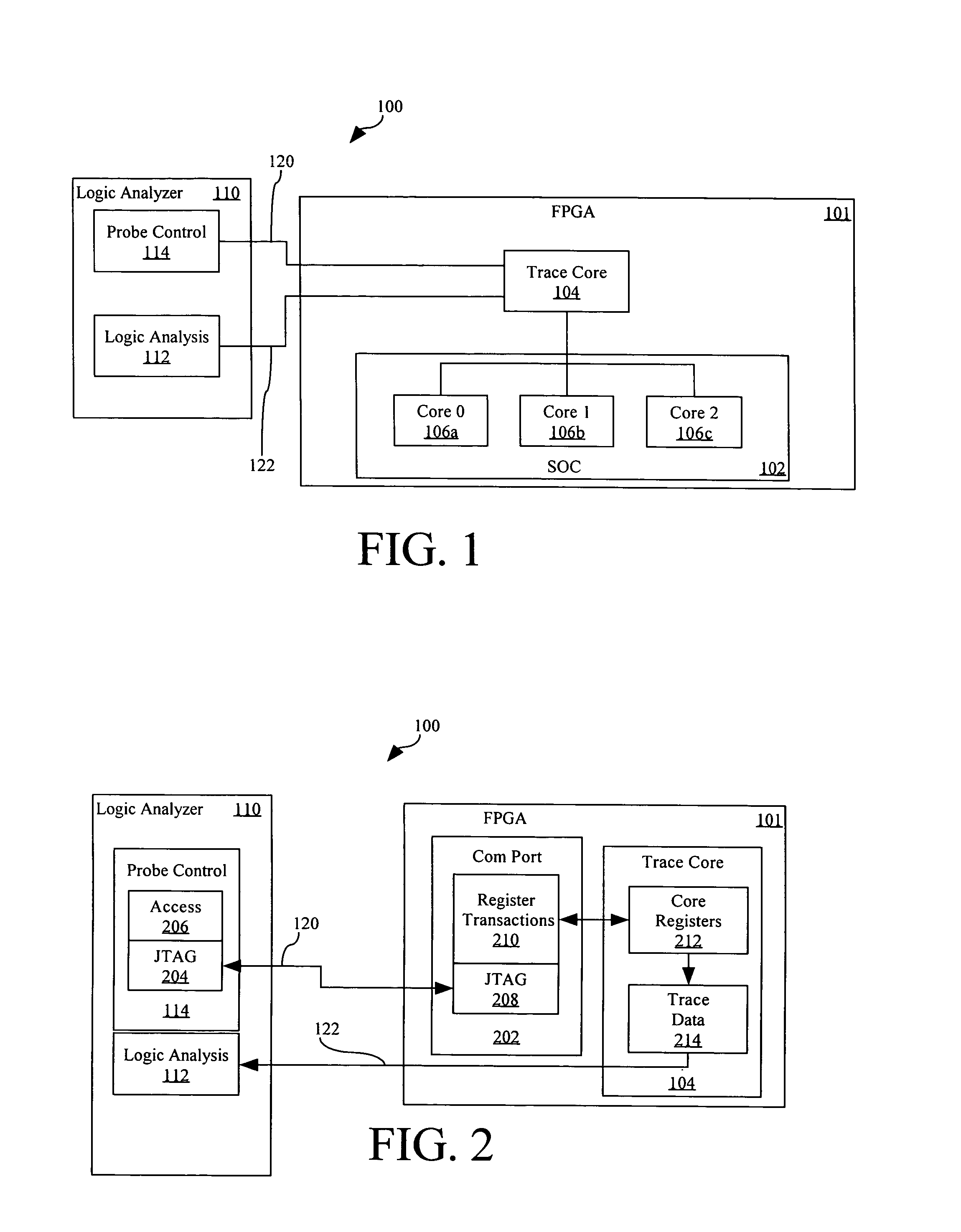
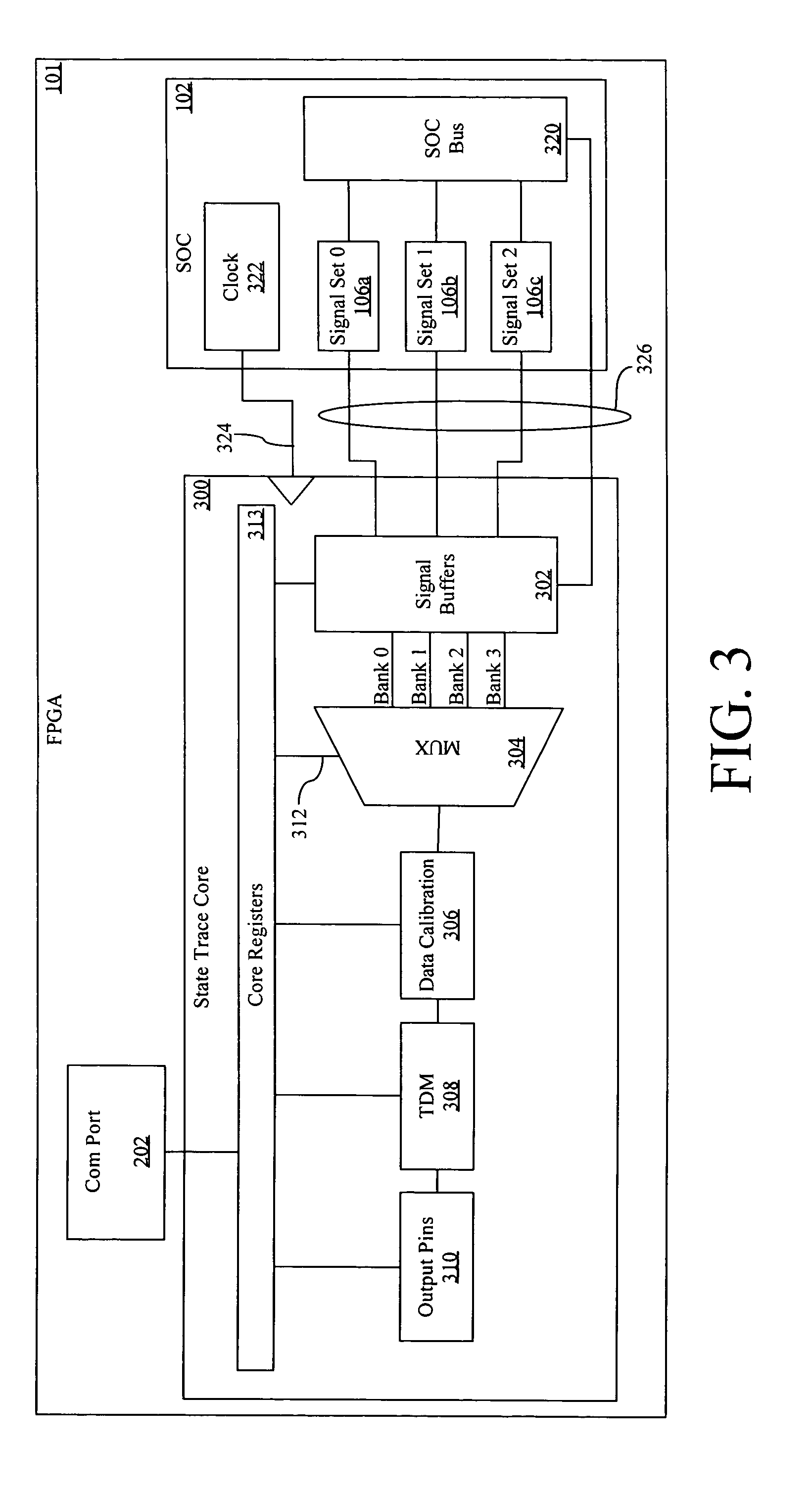
[0023]Reference will now be made in detail to the present invention, examples of which are illustrated in the accompanying drawings, wherein like reference numerals refer to like elements throughout. The detailed description which follows presents methods that may be embodied by routines and symbolic representations of operations of data bits within a computer readable medium, associated processors, logic analyzers, digital storage oscilloscopes, general purpose personal computers configured with data acquisition cards and the like. A routine is here, and generally, conceived to be a sequence of steps or actions leading to a desired result, and as such, encompasses such terms of art as “program,”“objects,”“functions,”“subroutines,” and “procedures.” These descriptions and representations are the means used by those skilled in the art effectively convey the substance of their work to others skilled in the art.

[0024]The apparatus and methods of the present invention will be described ...


PUM


Abstract

A dynamic probe system for probing a FPGA with at least one core. A trace core is added to the FPGA, the trace core in communication with a plurality of signal banks, each signal bank comprising a plurality of signals in the at least one core. A logic analyzer, in communication with the trace core and selecting the bank of signal to be sent from the trace core to the logic analyzer.

Description

BACKGROUND OF THE INVENTION[0001]A system on a chip, SOC, is designed using high level design units. These units, also known as cores or macros, are created in-house or purchased from a third party. Examples of cores include: embedded processors; busses; memory; external IO; and custom logic. The ideal in-house core is one that is complete and fully verified prior to using it in an SOC. If the core is not available, a third party core is sought. The third party core is a highly specialized intellectual property core that ideally plugs into the SOC design. If all the cores are functionally correct and they work well with each other, then the process of creating SOCs simply involves connecting cores together. However the reality is that this is usually not the case and most designs require extensive in-circuit testing.[0002]When doing in-circuit testing, the desired goal is to feed the chip with real world stimuli throughout the operating range; this type of testing is commonly called...

Claims


Application Information

Patent Timeline
Patent Type & Authority Patents(United States)
IPC IPC(8): G01R31/3177G01R31/40
CPCG01R31/3177G01R31/318519G01R31/3191G06F11/24G01R31/318533
Inventor WOODWARD, JOEL DHERNANDEZ, ADRIAN MSTEWART, III, JAMES B
Owner KEYSIGHT TECH
Why Eureka
Try Eureka