Semiconductor device comprising through-electrode interconnect

a technology of through electrodes and semiconductor devices, which is applied in the direction of semiconductor devices, semiconductor/solid-state device details, electrical apparatus, etc., can solve the problems of reliability degradation, inability to provide interconnections or the like in the region of through electrodes, etc., and achieves excellent insulating characteristics of surfaces, simple process, and high selectivity

Active Publication Date: 2009-06-02
RENESAS ELECTRONICS CORP
View PDF9 Cites 53 Cited by
  • Summary
  • Abstract
  • Description
  • Claims
  • Application Information

AI Technical Summary

Benefits of technology

[0011]In the semiconductor device of the present invention, the first conductive plug with smaller cross sectional area than the second conductive plug is disposed at the side of the main face, therefore, it is possible to enhance integration density of the interconnect in the vicinity of the through electrode. For this reason, the configuration is suitable for miniaturization.
[0046]As illustrated above according to the present invention, the through electrode is composed of the first conductive plug provided on the main face side and the second conductive plug whose cross sectional area is larger than that of the first conductive plug of the semiconductor substrate, therefore, there is provided the semiconductor device having the through electrode that is excellent in performance as for the electrode and the manufacturing stability.

Problems solved by technology

On the other hand, the through electrode described in the Japanese Laid-Open Patent Publication No. 2000-311982 has structure in which thick through electrode is penetrated through the semiconductor chip substrate, so that it is not possible to provide interconnect or the like on a region at which the through electrode is formed.
Further, there is a fear that reliability of the element deteriorates at the time the through electrode is formed because the through electrode is formed after forming elements.

Method used


Image

  • Semiconductor device comprising through-electrode interconnect
  • Semiconductor device comprising through-electrode interconnect
  • Semiconductor device comprising through-electrode interconnect

Examples


first embodiment

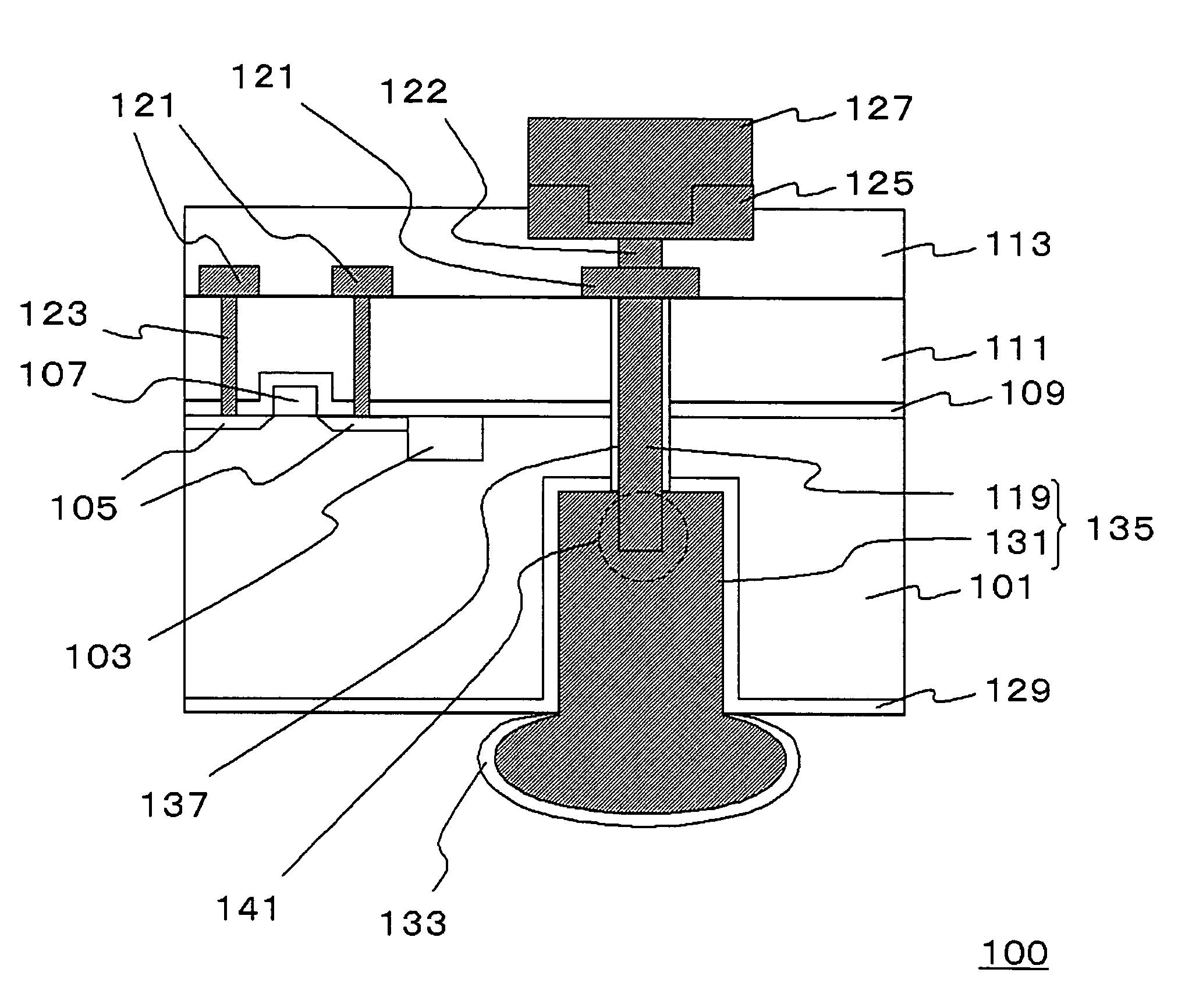
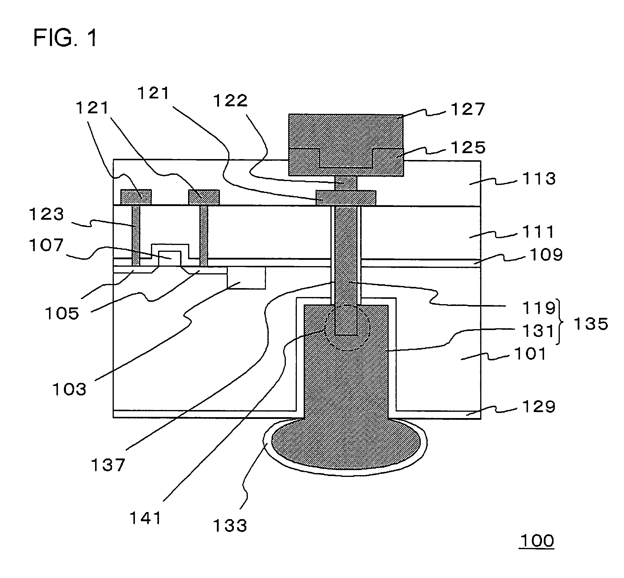
[0062]FIG. 1 is a cross-sectional view schematically showing configuration of a semiconductor device according to the present embodiment. The semiconductor device 100 of FIG. 1 has a layered structure formed with a silicon substrate 101, an etching stopper film 109, a lowermost layer insulating film 111, and a first interconnect layer insulating film 113. The semiconductor device 100 is provided with a through electrode 135 penetrating the silicon substrate 101, the etching stopper film 109 and the lowermost layer insulating film 111.

[0063]A MOS transistor composed of a diffusion layer 105, a gate electrode 107 and the like, and an isolation film 103 is formed on a main face of the silicon substrate 101. The lowermost layer insulating film 111 is formed so as to embed the MOS transistor and the isolation film 103. The etching stopper film 109 is provided in the lowermost insulating film 111 in such a way as to come into contact with an upper face of the silicon substrate 101 and the...

second embodiment

[0115]FIG. 3 is a cross-sectional view schematically showing a configuration of the semiconductor device according to the present embodiment. In the semiconductor device 102 shown in FIG. 3, the upper face of the large diameter plug 131 matches the upper face of the silicon substrate 101, that is, the main face of the silicon substrate 101. In addition, in the semiconductor device 102, SiN film 143 is formed on a side face of the large diameter plug 131 and SiN film 145 is formed on a rear surface of the silicon substrate 101 instead of the electrodeposited insulating film 129 in the silicon substrate 101 shown in FIG. 1.

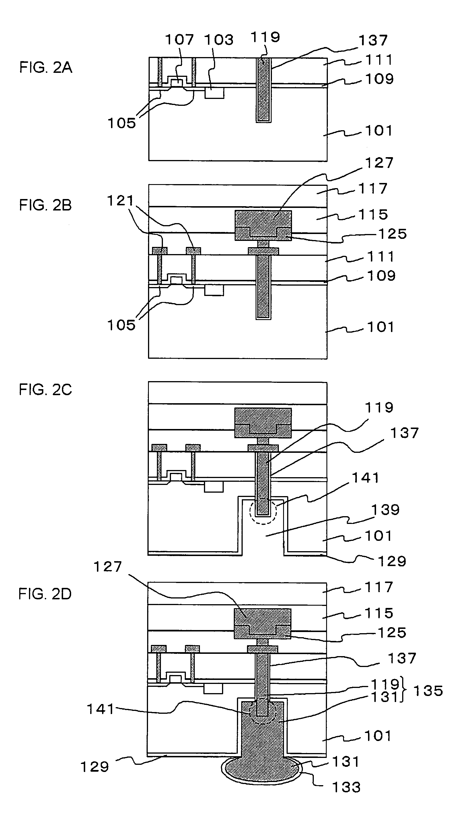
[0116]Next, there will be illustrated a method for manufacturing the semiconductor device 102. FIGS. 4A to 4D are cross-sectional views schematically showing the manufacturing process of the semiconductor device 102 shown in FIG. 2.

[0117]Firstly, a resist pattern (not shown in the drawings) having an opening corresponding to the shape of the large diameter plug 131 ...

third embodiment

[0136]FIG. 5 is a cross-sectional view schematically showing a configuration of the semiconductor device according to the present embodiment. In a semiconductor device 104 shown in FIG. 5, there is provided an SiO2 ring 151 to cover the periphery of the large diameter plug 131. The SiO2 ring 151 is provided in such a way as to come into contact with the SiN film 143 in the side face of the large diameter plug 131. The side face of the SiO2 ring 151 comes into contact with the silicon substrate 101 via the SiN film 143. In addition, like the second embodiment, the SiN film 149 is provided on the rear surface of the silicon substrate 101.

[0137]Next, there will be described a method for manufacturing the semiconductor device 104. FIGS. 6A to 6D are cross-sectional views schematically showing the manufacturing process of the semiconductor device 104 shown in FIG. 5.

[0138]Firstly, the configuration shown in FIG. 6A is formed. At the beginning, the antireflection film and the photoresist ...


PUM


Abstract

A semiconductor device having a through electrode excellent in performance as for an electrode and manufacturing stability is provided. There is provided a through electrode composed of a conductive small diameter plug and a conductive large diameter plug on a semiconductor device. A cross sectional area of the small diameter plug is made larger than a cross sectional area and a diameter of a connection plug, and is made smaller than a cross sectional area and a diameter of the large diameter plug. In addition, a protruding portion formed in such a way that the small diameter plug is projected from the silicon substrate is put into an upper face of the large diameter plug. Further, an upper face of the small diameter plug is connected to a first interconnect.

Description

[0001]This application is based on Japanese patent application NO. 2004-108304, the content of which is incorporated hereinto by reference.BACKGROUND OF THE INVENTION[0002]1. Field of the Invention[0003]The present invention related to a semiconductor device and a method for manufacturing the same.[0004]2. Related Art[0005]In recent years a semiconductor device necessitates to be lightweight, thin, and short sized, and a high performance. In the semiconductor device such as multi-chip package or the like, realizing high density interconnect, miniaturization of a logic chip and capacity increase of a memory is aggressively promoted.[0006]As for one corresponding medium coping with such proposals, it is tried that realizing high density interconnect or the like is achieved upon providing a through electrode on the semiconductor substrate. A through electrode as for the conventional one is described in the Japanese Laid-Open Patent Publication No. 2000-311982.[0007]The Japanese Laid-Op...

Claims


Application Information

Patent Timeline
Patent Type & Authority Patents(United States)
IPC IPC(8): H01L23/48H01L23/52H01L21/28H01L21/3205H01L21/44H01L21/60H01L21/768H01L21/8242H01L29/40
CPCH01L21/76898H01L23/481H01L24/11H01L2924/13091H01L2224/13099H01L2224/16H01L2924/01013H01L2924/01015H01L2924/01029H01L2924/01033H01L2924/01074H01L2924/01078H01L2924/01079H01L2924/01082H01L2924/04953H01L2924/10329H01L2924/19043H01L2924/30105H01L2924/01005H01L2924/01006H01L2924/01072H01L2924/014H01L2924/00H01L2224/05009H01L2224/05001H01L2224/05572H01L2224/05624H01L2224/05647H01L2224/05655H01L2224/13009H01L24/03H01L24/05H01L24/13H01L2924/00014
Inventor KAWANO, MASAYA
Owner RENESAS ELECTRONICS CORP
Why Eureka
Try Eureka