

Storage-capacitor electrode and interconnect
a storage capacitor and electrode technology, applied in the field of semiconductor memories, can solve the problems of reducing the operational efficiency of a dram is noise, reducing the operational efficiency of a dram, and causing the amplifier of a dram to output erroneous logic values,
- Summary
- Abstract
- Description
- Claims
- Application Information
AI Technical Summary
Benefits of technology
Problems solved by technology
Method used
Image

Examples
first embodiment
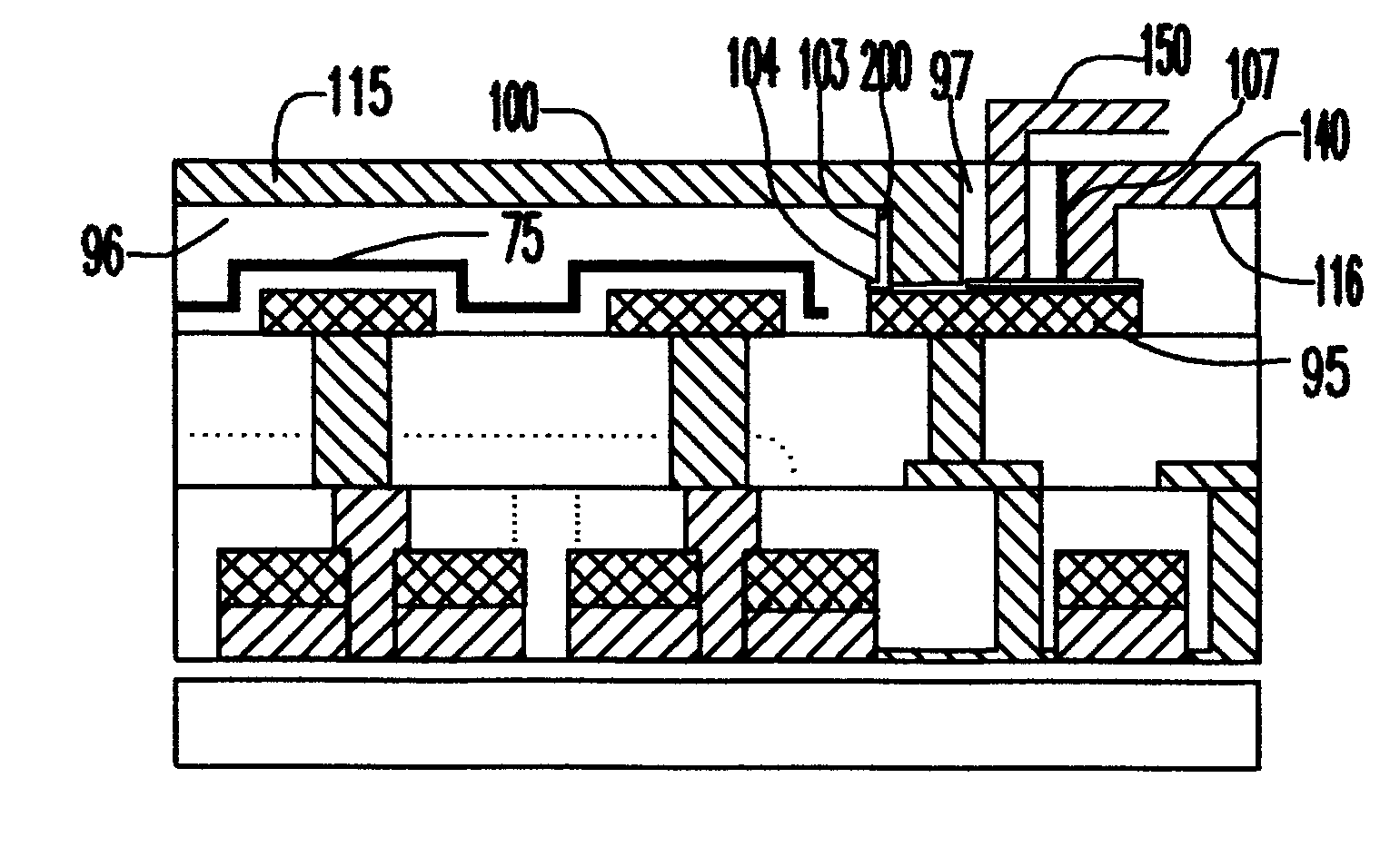
the method of the present invention, thus, forms a DRAM memory cell having an intermediate wiring level between metal layers (69,63) and 100. This intermediate wiring level includes at least one wiring layer in the form of lower capacitor electrode 72 which electrically connects metal layers 63 and 100.
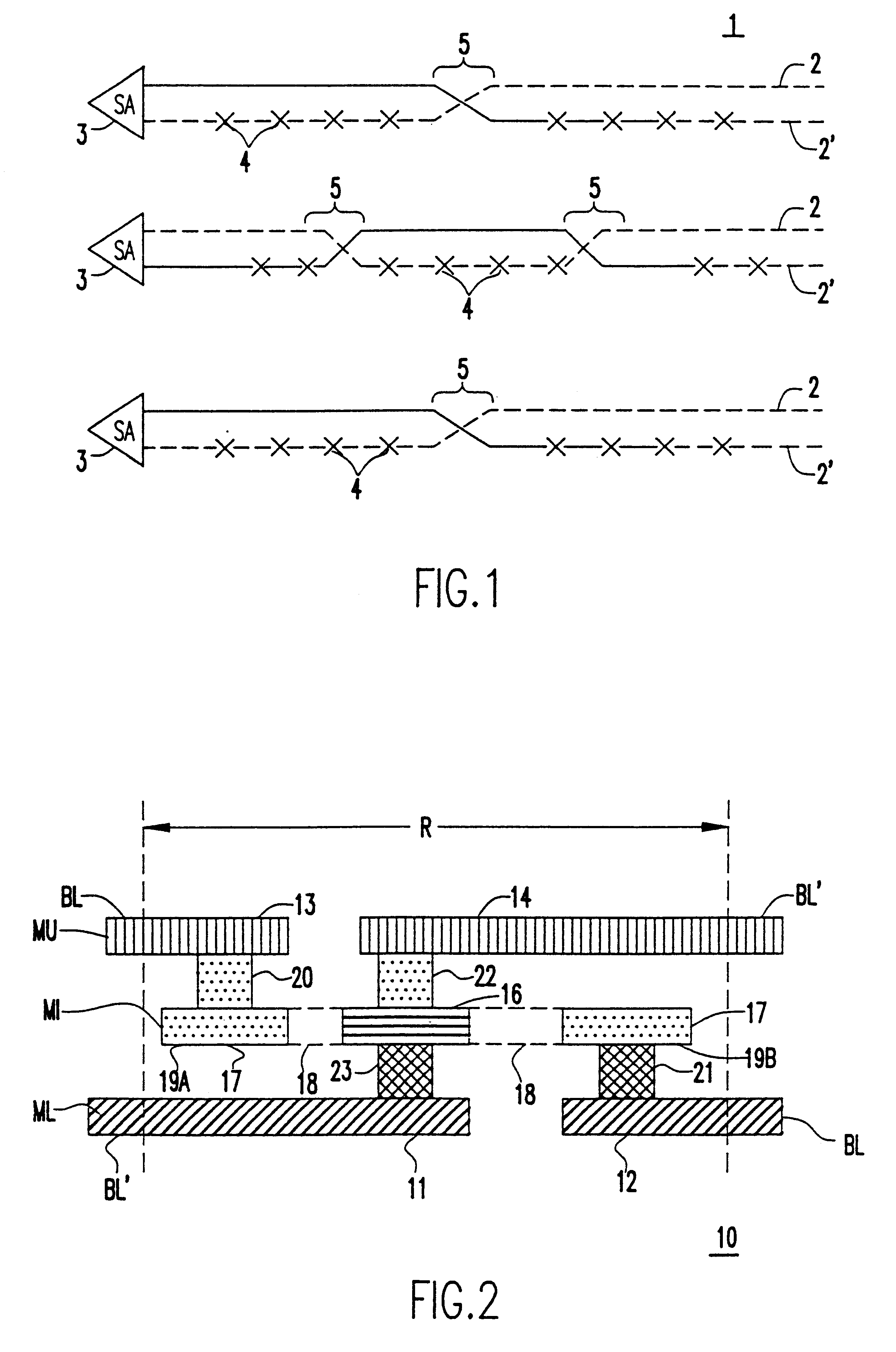
Metal layers 63 and 100 may be one of a variety chip features. For example, metal layers 63 and 100 may be portions of a bit line disposed on different levels of the DRAM structure. Under these circumstances, electrode 95 may advantageously be used to establish a flipped connection between these bit lines portions. Alternatively, metal layers 63 and 100 may be interconnects attached to one or more support circuits of the DRAM, which are then connected by electrode 72 through studs 97 and 64. Still further, electrode 72 may be used to connect support circuits to a diffusion region or gate electrodes in substrate 52 via elements 64, 63, and 62 where support device 54 may eventually rece...
second embodiment
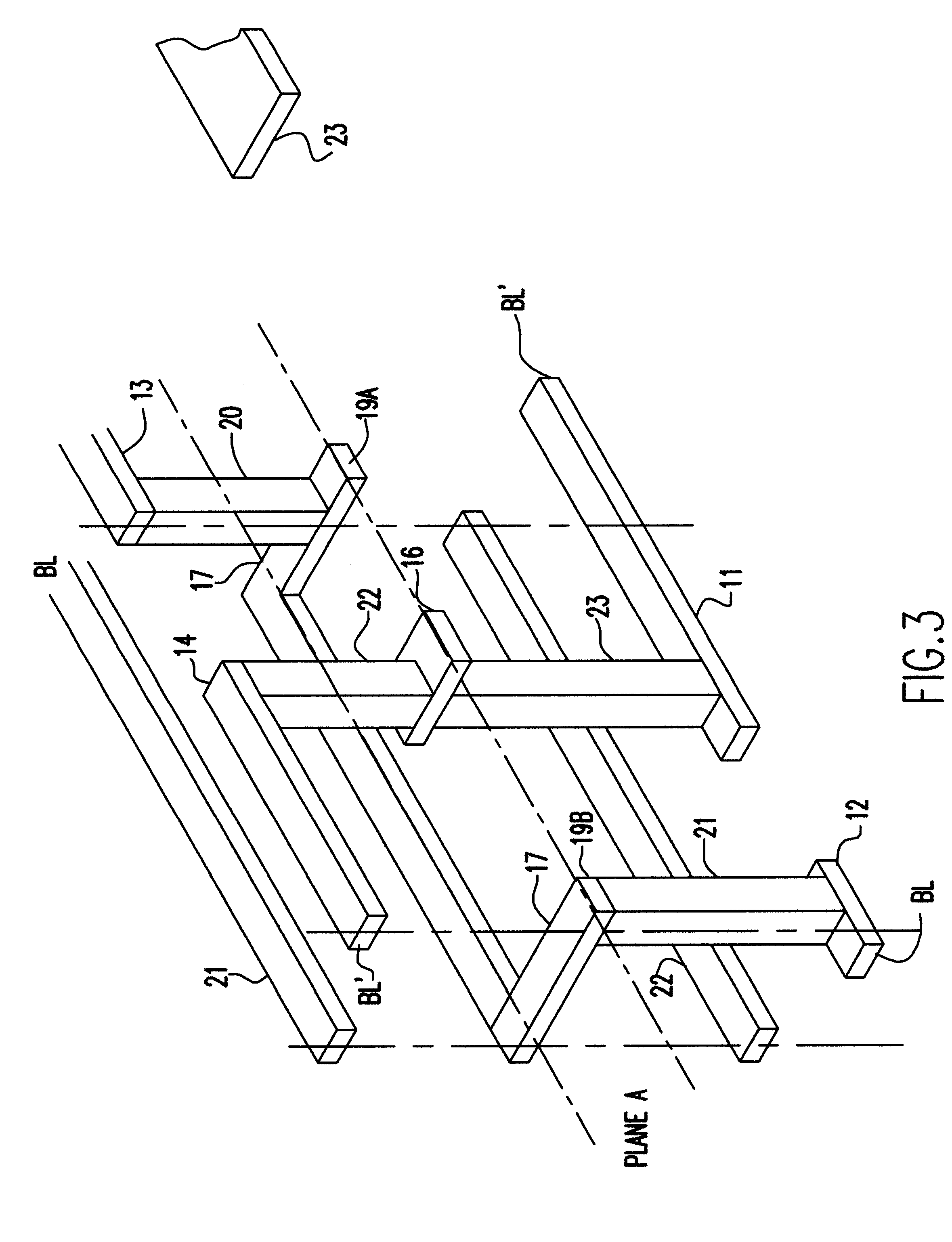
the present invention, thus, forms a DRAM memory cell structure having an intermediate wiring level between metal layers 63 and 100. This intermediate wiring level is in the form of a layered structure which includes lower capacitor electrode 72, dielectric 72, and upper capacitor electrode 120. In this embodiment, only lower capacitor electrode 95 is used to electrically connect metal layers 63 and 100, which may be bit-lines, support circuits interconnects, or any of the other types of interconnects and global wirings previously discussed. For example, the layered structure of the second embodiment especially well suited for use as either capacitor electrode 16 or 17 forming the flipped bit-line connections shown in FIGS. 2 and 3.
While the upper capacitor electrode 120 is not used as an interconnect in the second embodiment, it nevertheless is beneficial in a number of respects. For example, the upper capacitor electrode advantageously improves the planarity of the overlying diele...
third embodiment
the present invention, thus, forms a DRAM memory cell structure having an intermediate wiring level connecting metal layers 100 and 200. This intermediate wiring layer is in the form of a layered structure which includes lower capacitor electrode 95, dielectric 75, and upper capacitor electrode 120. In this embodiment, only upper electrode 120 is used to electrically connect metal layers 100 and 200, which may be support circuits interconnects or any of the other types of global wiring previously discussed.
For all embodiments herein, the upper capacitor electrode may be made from platinum (Pt) and the dielectric from (Ba,Sr)TiO.sub.3. In selecting these materials, it is noted that there are usually more constraints placed on the choice of materials for the lower electrode than on the upper electrode, for example, because the lower electrode must be able to withstand high temperature annealing. A refractory metal (e.g., one having a high melting point), therefore, is usually selected...
PUM
 Abstract
Description
Claims
Application Information