Storage node, phase change memory device and methods of operating and fabricating the same

a phase change memory and storage node technology, applied in the direction of semiconductor memory devices, electrical appliances, basic electric elements, etc., can solve the problems of deterioration of production yield and reliability of prams, and achieve the effects of increasing the integration density of prams, and reducing the amount of peltier hea

Inactive Publication Date: 2007-05-17
SAMSUNG ELECTRONICS CO LTD
View PDF2 Cites 43 Cited by
  • Summary
  • Abstract
  • Description
  • Claims
  • Application Information

AI Technical Summary

Benefits of technology

[0031] According to example embodiments, a reset current may be reduced in accordance with an increased amount of Peltier heat by Peltier effect. Because an allowable current for a transistor may be reduced, a size of the transistor may be further scaled down, thereby providing an effect of increasing an integration density of a PRAM. According to example embodiments, the reduction of the reset current may be caused by Peltier heat, and may not be related with a size reduction of the lower electrode contact layer. According to example embodiments, an integration density of a PRAM may be increased without an increase of a set resistance.

Problems solved by technology

Because the methods also increase the set resistance, a production yield and a reliability of the PRAM may be deteriorated.

Method used


Image

  • Storage node, phase change memory device and methods of operating and fabricating the same
  • Storage node, phase change memory device and methods of operating and fabricating the same
  • Storage node, phase change memory device and methods of operating and fabricating the same

Examples


Embodiment Construction

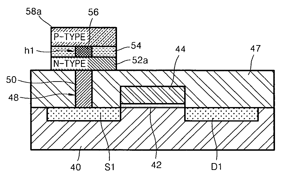
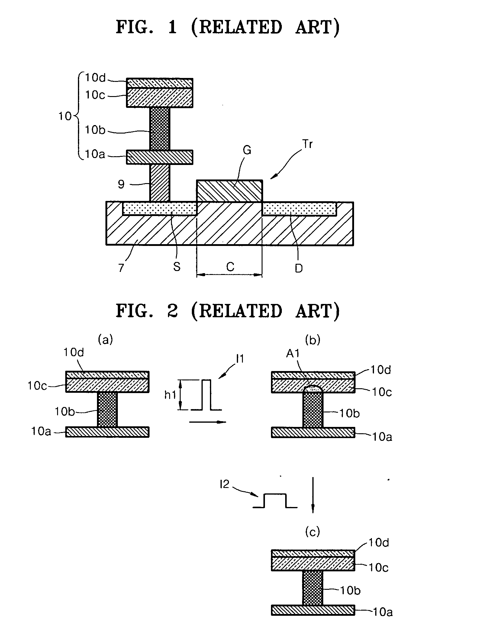
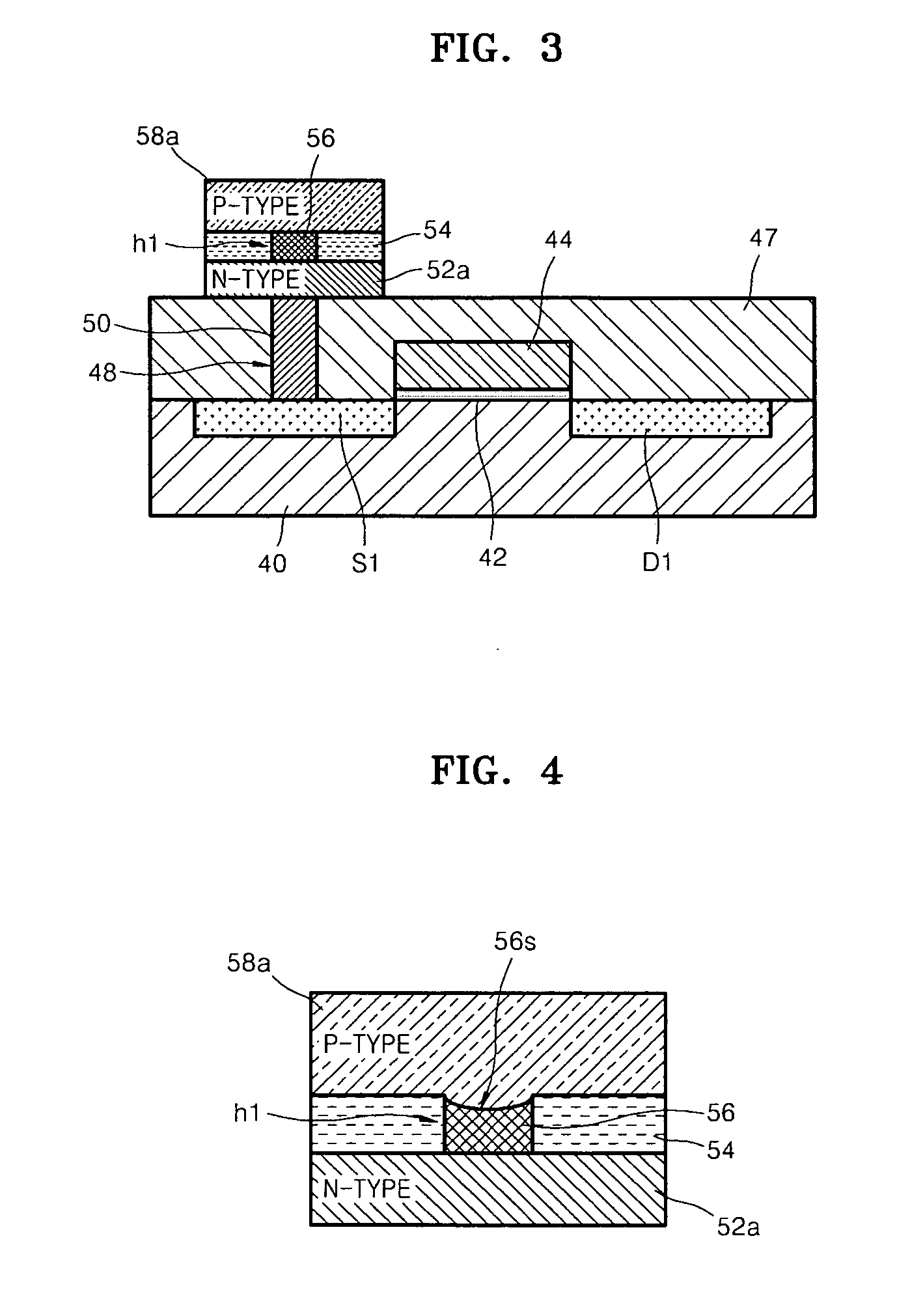
[0042] Example embodiments will now be described more fully hereinafter with reference to the accompanying drawings, in which example embodiments are shown. Example embodiments may, however, be embodied in many different forms and should not be construed as being limited to the embodiments set forth herein. Rather, these embodiments are provided so that this disclosure will be thorough and complete, and will fully convey the scope of example embodiments to those skilled in the art. Like numbers refer to like elements throughout the specification.

[0043] Hereinafter, a phase change memory device, and methods of operating and fabricating the same according to example embodiments will be explained in detail with reference to attached drawings. In the drawings, the thicknesses of layers and regions are exaggerated for clarity.

[0044] It will be understood that when an element or layer is referred to as being “on,”“connected to” or “coupled to” another element or layer, it can be directl...


PUM

PropertyMeasurementUnit
thicknessaaaaaaaaaa
thicknessaaaaaaaaaa
diameteraaaaaaaaaa

Abstract

A storage node, a phase change memory device, and methods of operating and fabricating the same are provided. The storage node may include a lower electrode, a phase change layer on the lower electrode and an upper electrode on the phase change layer, and the lower electrode and the upper electrode may be composed of thermoelectric materials having a melting point higher than that of the phase change layer, and having different conductivity types. An upper surface of the lower electrode may have a recessed shape, and a lower electrode contact layer may be provided between the lower electrode and the phase change layer. A thickness of the phase change layer may be about 100 nm or less, and the lower electrode may be composed of an n-type thermoelectric material, and the upper electrode may be composed of a p-type thermoelectric material, or they may be composed on the contrary to the above. Seeback coefficients of the lower electrode, the phase change layer, and the upper electrode may be different from each other.

Description

PRIORITY STATEMENT [0001] This application claims priority under 35 USC § 119 to Korean Patent Application No. 10-2005-0102499, filed on Oct. 28, 2005, in the Korean Intellectual Property Office (KIPO), the entire contents of which are incorporated herein by reference. BACKGROUND [0002] 1. Field [0003] Example embodiments relate to a storage node, a semiconductor memory device and methods of operating and fabricating the same. Other example embodiments relate to a storage node, a phase change memory device and methods of operating and fabricating the same. [0004] 2. Description of the Related Art [0005] A phase change random access memory (PRAM) may be one of non-volatile memory devices (e.g., a flash memory, a ferroelectric random access memory (FRAM) and / or a magnetic random access memory (MRAM)). A difference of a PRAM and other non-volatile memory devices may be a structure of a storage node. The storage node of a PRAM may include a phase change layer. A phase of the phase chang...

Claims


Application Information

Patent Timeline
Patent Type & Authority Applications(United States)
IPC IPC(8): H01L29/94
CPCH01L27/2436H01L45/06H01L45/1233H01L45/1286H01L45/144H01L45/1675H01L45/1683H10B63/30H10N70/231H10N70/826H10N70/8613H10N70/8828H10N70/063H10N70/066
Inventor SUH, DONG-SEOKPARK, TAE-SANG
Owner SAMSUNG ELECTRONICS CO LTD
Why Eureka
Try Eureka