Integrated circuits and methods of forming the same

Active Publication Date: 2011-12-08
TAIWAN SEMICON MFG CO LTD
View PDF2 Cites 33 Cited by
  • Summary
  • Abstract
  • Description
  • Claims
  • Application Information

AI Technical Summary

Problems solved by technology

Such two-dimensional (2D) integration density improvements are physically limited by device size, the size of the die, and other limitations including the complexity of design, such as, for example, the requisite length and number of interconnections between devices, and the corresponding circuit delay and power consumption increases.
As the substrate resistivity decreases, the eddy currents that can circulate in the substrat

Method used


Image

  • Integrated circuits and methods of forming the same
  • Integrated circuits and methods of forming the same
  • Integrated circuits and methods of forming the same

Examples


Embodiment Construction

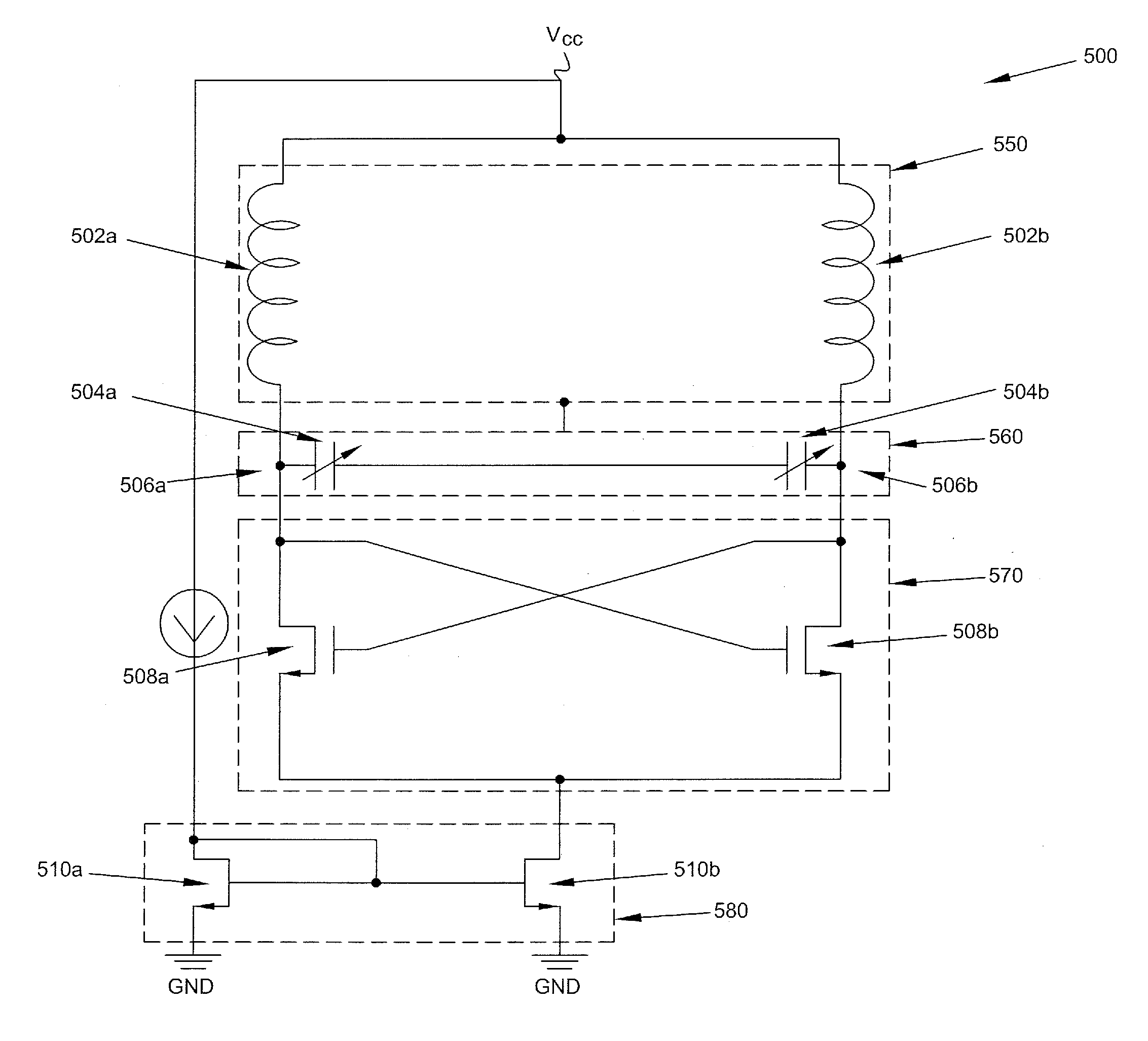
[0021]With reference to the Figures where like elements have been given like numerical designations to facilitate an understanding of the present invention, the various embodiments of a varactor and method of forming the same is provided.

[0022]With reference to FIG. 3, a cross-sectional view of a three-dimensional integrated circuit design according to an embodiment of the present disclosure is shown. The integrated circuit 300 includes a substrate 330. In some embodiments, the substrate 330 is a semiconductor wafer. In another embodiment, the substrate is a semiconductor die. In an embodiment, the substrate 330 may be a p-type substrate. The substrate 330 may be formed from a material including, but not limited to, a Group IV elemental or compound semiconductor or a Group III-V semiconductor. The substrate 330 may include silicon. The substrate 330 may include another elementary semiconductor such as, for example, germanium. The substrate 330 may also include a compound semiconduct...


PUM


Abstract

A three-dimensional integrated circuit includes a semiconductor substrate where the substrate has an opening extending through a first surface and a second surface of the substrate and where the first surface and the second surface are opposite surfaces of the substrate. A conductive material substantially fills the opening of the substrate to form a conductive through-substrate-via (TSV). An active circuit is disposed on the first surface of the substrate, an inductor is disposed on the second surface of the substrate and the TSV is electrically coupled to the active circuit and the inductor. The three-dimensional integrated circuit may include a varactor formed from a dielectric layer formed in the opening of the substrate such that the conductive material is disposed adjacent the dielectric layer and an impurity implanted region disposed surrounding the TSV such that the dielectric layer is formed between the impurity implanted region and the TSV.

Description

FIELD OF THE INVENTION[0001]The present disclosure is directed generally to integrated circuits. In particular, the present disclosure relates to integrated circuit structures including through-substrate-vias.DESCRIPTION OF THE RELATED ART[0002]Developments in integrated circuit technology have often focused on improving the integration density of various electronic components (e.g. transistors, capacitors, diodes, resistors, inductors, etc.) into a given chip or wafer area. Various improvements have involved the reduction of minimum component size, permitting more components to be integrated on the surface of the semiconductor die. Such two-dimensional (2D) integration density improvements are physically limited by device size, the size of the die, and other limitations including the complexity of design, such as, for example, the requisite length and number of interconnections between devices, and the corresponding circuit delay and power consumption increases.[0003]Three-dimensio...

Claims


Application Information

Patent Timeline
IPC IPC(8): H03B5/12H01L21/329H01L29/93
CPCH01L29/93H01L27/016
Inventor YEN, HSIAO-TSUNGHU, HSIEN-PINLU, JHE-CHINGKUO, CHIN-WEICHEN, MING-FALIU, SALLY
Owner TAIWAN SEMICON MFG CO LTD
Why Eureka
Try Eureka