Methods of forming multi-level cell of semiconductor memory

a semiconductor memory and multi-level technology, applied in the field of non-volatile memory devices, can solve the problems of limiting the number of repeated data storage, requiring a relatively high voltage for data storage, and all stored data is lost, so as to achieve the effect of improving the integration density

Active Publication Date: 2010-04-15
SAMSUNG ELECTRONICS CO LTD
View PDF8 Cites 41 Cited by
  • Summary
  • Abstract
  • Description
  • Claims
  • Application Information

AI Technical Summary

Benefits of technology

[0008]Exemplary embodiments provide a method of forming a multi-level cell of a semiconductor memory capable of storing more data in a unit memory cell without increasing the number of memory cells in order to enhance integration density.

Problems solved by technology

However, when power is cut off, all stored data is lost.
However, the flash memory device has certain drawbacks, such as requiring a relatively high voltage for data storage and limiting the number of repeated data storage.

Method used


Image

  • Methods of forming multi-level cell of semiconductor memory
  • Methods of forming multi-level cell of semiconductor memory
  • Methods of forming multi-level cell of semiconductor memory

Examples


Embodiment Construction

[0031]Various exemplary embodiments will now be described more fully with reference to the accompanying drawings in which some exemplary embodiments are shown. This inventive concept may, however, be embodied in different forms and should not be construed as limited to the embodiments set forth herein. Rather, these embodiments are provided so that this description is thorough and complete and fully conveys the invention to one skilled in the art. It will be understood that although the terms, such as “first,”“second” and the like, are used herein to describe various elements, the elements should not be limited by these terms. These terms are only used to distinguish one element from another element.

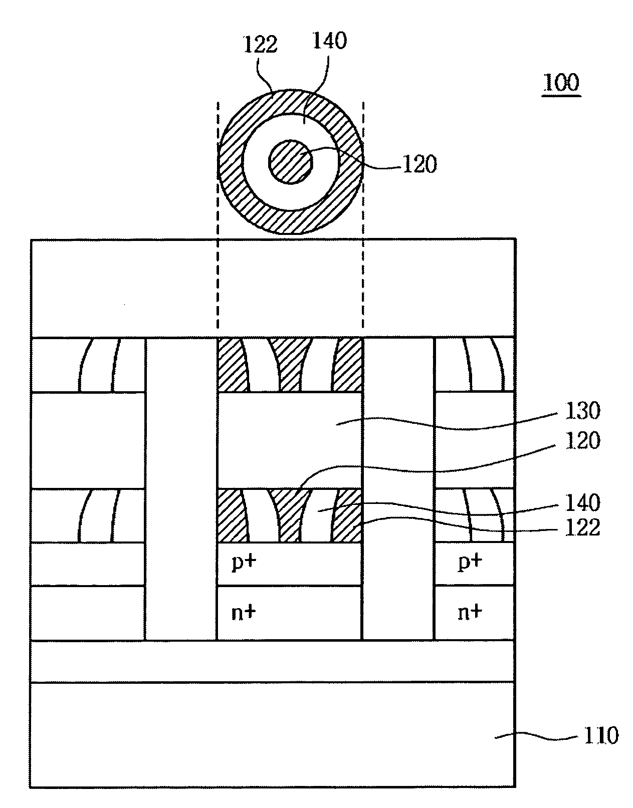
[0032]A method of forming a multi-level cell of a semiconductor memory according to the inventive concept will be described in detail below with reference to the accompanying drawings.

[0033]The exemplary embodiment of the inventive concept relates to a non-volatile memory device that doe...


PUM


Abstract

Provided is a method of forming a semiconductor memory cell in which in order to store two bits or more data in a memory cell, three or more bottom electrode contacts (BECs) and phase-change materials (GST) have a parallel structure on a single contact plug (CP) and set resistances are changed depending on thicknesses (S), lengths (L) or resistivities (ρ) of the three or more bottom electrode contacts, so that a reset resistance and three different set resistances enable data other than in set and reset states to be stored. Also, a method of forming a memory cell in which three or more phase-change materials (GST) have a parallel structure on a single bottom electrode contact, and the phase-change materials have different set resistances depending on composition ratio or type, so that four or more different resistances can be implemented is provided.

Description

CROSS-REFERENCE TO RELATED APPLICATION[0001]This application claims the benefit of Korean Patent Application No. 10-2008-0100174, filed in the Korean Intellectual Property Office Oct. 13, 2008, the contents of which are hereby incorporated herein by reference in their entirety.BACKGROUND[0002]1. Field[0003]Exemplary embodiments relate to a non-volatile memory device which has a resistance which is variable depending upon a current or voltage and which need not be refreshed since stored data is retained even when power is cut off, and more particularly, to a method of forming a multi-level cell in which a bottom electrode contact (BEC) or a phase-change material (GST) has three or more parallel structures, so that two or more bits of data are stored in a memory cell.[0004]2. Description of Related Art[0005]A semiconductor memory device requires high operating speed and drivability at low power and a large number of memory cells per unit area, i.e., high integration density. Much rese...

Claims


Application Information

Patent Timeline
Patent Type & Authority Applications(United States)
IPC IPC(8): H01L21/06
CPCH01L27/2409H01L45/06H01L45/1233H01L45/1253H01L45/1683H01L45/143H01L45/144H01L45/1666H01L45/141H10B63/20H10N70/231H10N70/841H10N70/882H10N70/826H10N70/8828H10N70/061H10N70/066H01L21/31051H01L21/76229H10N70/8825
Inventor OH, GYU-HWANAN, HYEONG-GEUNPARK, SOON-OHAHN, DONG-HOPARK, YOUNG-LIM
Owner SAMSUNG ELECTRONICS CO LTD
Why Eureka
Try Eureka