Methods of fabricating three-dimensional semiconductor memory devices

a semiconductor memory and three-dimensional technology, applied in the direction of semiconductor devices, basic electric elements, electrical equipment, etc., can solve the problems of limited application and practical limitations of increasing integration density, and the need for process equipment to increase pattern fineness, so as to improve reliability and increase integration density

Active Publication Date: 2012-11-22
SAMSUNG ELECTRONICS CO LTD
View PDF6 Cites 43 Cited by
  • Summary
  • Abstract
  • Description
  • Claims
  • Application Information

AI Technical Summary

Benefits of technology

[0006]Example embodiments of the inventive concepts may provide methods of fabricating three dimensional semiconductor memory devices with increased integration density and improved reliability.

Problems solved by technology

However, the extremely expensive process equipment needed to increase pattern fineness sets a practical limitation on increasing integration density of two-dimensional or planar semiconductor memory devices.

Method used


Image

  • Methods of fabricating three-dimensional semiconductor memory devices
  • Methods of fabricating three-dimensional semiconductor memory devices
  • Methods of fabricating three-dimensional semiconductor memory devices

Examples


Embodiment Construction

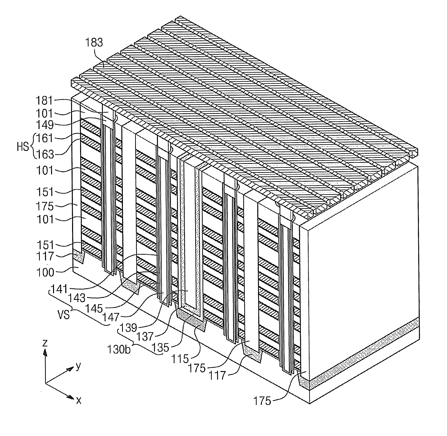
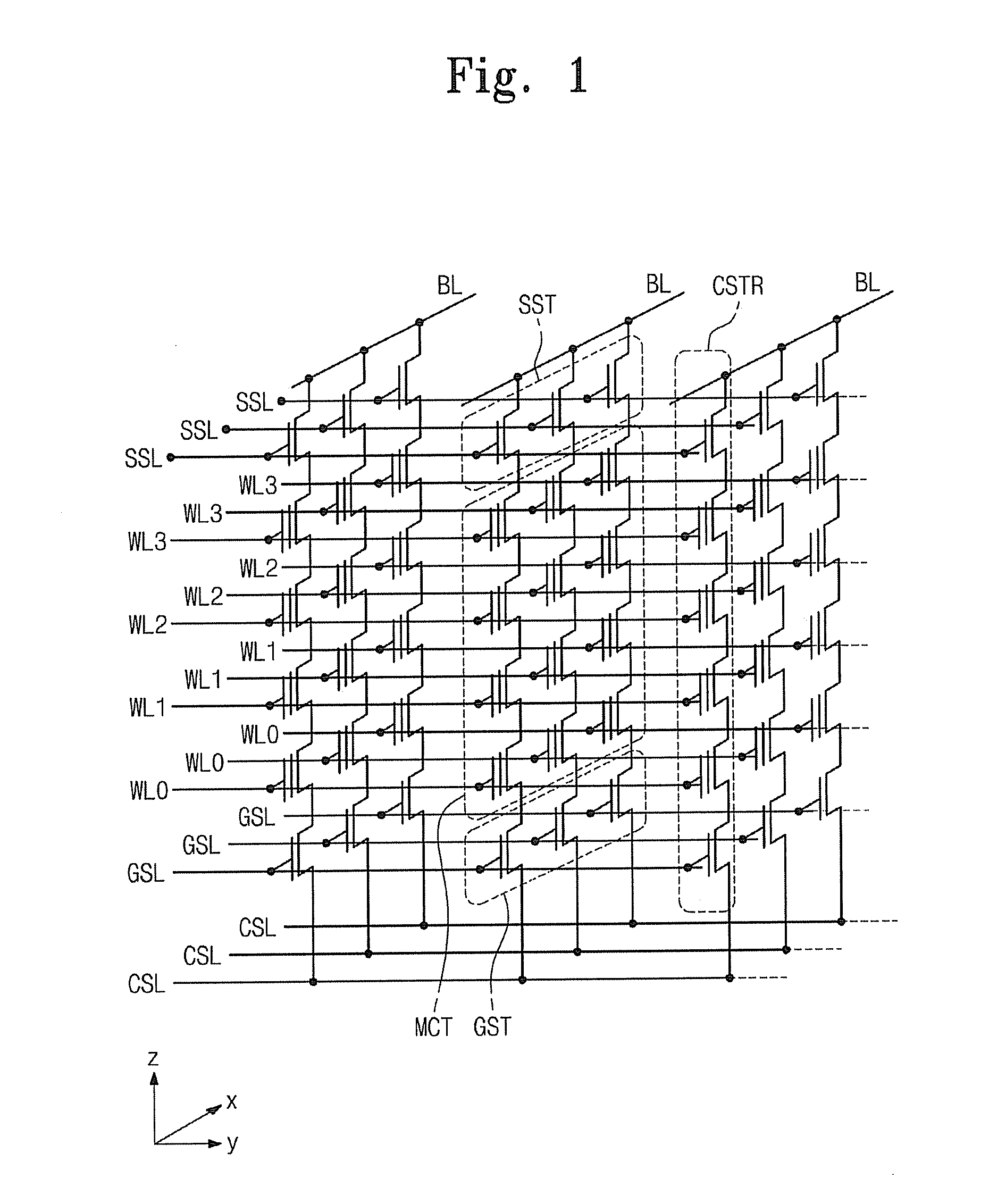
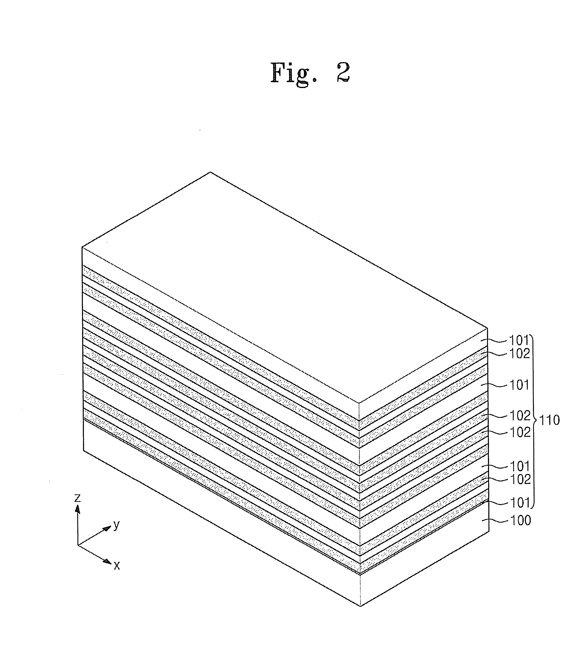
[0023]Example embodiments of the inventive concepts will now be described more fully with reference to the accompanying drawings, in which example embodiments are illustrated. Example embodiments of the inventive concepts may, however, be embodied in many different forms and should not be construed as being limited to the embodiments set forth herein; rather, these embodiments are provided so that this disclosure will be thorough and complete, and will fully convey the concept of example embodiments to those of ordinary skill in the art. In the drawings, the thicknesses of layers and regions are exaggerated for clarity. Like reference numerals in the drawings denote like elements, and thus their description will be omitted.

[0024]It will be understood that when an element is referred to as being “connected” or “coupled” to another element, it can be directly connected or coupled to the other element or intervening elements may be present. In contrast, when an element is referred to a...


PUM


Abstract

Methods of fabricating three-dimensional semiconductor memory devices including forming a plate stack structure with insulating layers and sacrificial layers stacked alternatingly on a substrate, forming first and second trenches separating the plate stack structure into a plurality of mold structures, the first trench being between the second trenches, forming first vertical insulating separators in the first and second trenches, forming semiconductor patterns penetrating the mold structure and being spaced apart from the first and second trenches, removing the first vertical insulating separator from the second trench to expose the sacrificial layers, removing the sacrificial layers exposed by the second trench to form recess regions partially exposing the semiconductor patterns and the first vertical insulating separator, and forming conductive patterns in the recess regions.

Description

CROSS-REFERENCE TO RELATED APPLICATION[0001]This U.S. non-provisional patent application claims priority under 35 U.S.C. §119 to Korean Patent Application No. 10-2011-0047445, filed on May 19, 2011, in the Korean Intellectual Property Office (WO), the entire contents of which are incorporated herein by reference.BACKGROUND OF THE INVENTION[0002]1. Field[0003]Example embodiments of the inventive concepts relate generally to methods of fabricating semiconductor memory devices. More particularly, example embodiments of the inventive concepts relate to methods of fabricating three dimensional semiconductor memory devices including vertically stacked memory cells.[0004]2. Description of the Related Art[0005]In typical two-dimensional or planar semiconductor memory devices, integration density is mainly determined by the area occupied by a unit memory cell, and integration density is greatly influenced by the level of a fine pattern forming technology. However, the extremely expensive pro...

Claims


Application Information

Patent Timeline
Patent Type & Authority Applications(United States)
IPC IPC(8): H01L21/336H01L21/31H01L21/28H01L21/302
CPCH01L29/7926H01L27/11582H10B43/27H01L21/76205H01L27/0688H01L21/31
Inventor YUN, JUMIPARK, KWANGMINYOO, DONGCHULJANG, BYONG-HYUN
Owner SAMSUNG ELECTRONICS CO LTD
Why Eureka
Try Eureka