FPGA equivalent input and output grid muxing on structural ASIC memory

a technology of asic memory and input and output grid, applied in the field of switching or multiplexing structures, can solve the problems of increasing the loading of input and output muxing paths, complex design, and large layout area, and achieve the effect of efficiently transmitting signals

Inactive Publication Date: 2009-06-02
ALTERA CORP
View PDF5 Cites 8 Cited by
  • Summary
  • Abstract
  • Description
  • Claims
  • Application Information

AI Technical Summary

Benefits of technology

[0006]Accordingly, embodiments of the present invention provide circuits, methods, and apparatus directed to an integrated circuit having a memory interface that is configurable to have one of a multiple different bus widths. The memory interface is compact and transmits signals efficiently. In one embodiment, the memory interface has a first set of lines and a second set of lines. The first set of lines may be organized to have a first orientation and the second set of lines to have a second orientation. The first and second set of lines are arranged such that there are multiple locations at which a via may be placed to connect a line of the first set to a line of the second set. The placement of the vias determines the bus width of the memory interface. In one embodiment, there are a greater number of locations than vias that are placed.

Problems solved by technology

However, directly transferring the multiple bus width configurations from the FPGA to the corresponding ASIC would degrade performance by leading to a bigger layout area, a more complex design, and an increased loading on the input and output muxing paths.
Accordingly, when the FPGA has the flexibility of multiple bus width configurations, it is not desirable to directly transfer the multiple data bus width configurations from the FPGA to the corresponding ASIC.
Such direct transferring would at least partially defeat the purpose of having an ASIC, which is designed to be smaller and faster than the FPGA.

Method used


Image

  • FPGA equivalent input and output grid muxing on structural ASIC memory
  • FPGA equivalent input and output grid muxing on structural ASIC memory
  • FPGA equivalent input and output grid muxing on structural ASIC memory

Examples


Embodiment Construction

[0021]Embodiments of the present invention are directed to methods and multiplexing (muxing) structures used, for example, to send data to or retrieve data from a memory module or other circuit element along data buses of different widths. Generally, the data is produced by a structured application-specific integrated circuit (ASIC). However, one skilled in the art will appreciate that embodiments of the invention may be applied to other types of integrated circuits and that the transmission of data along the data bus need not involve a memory module.

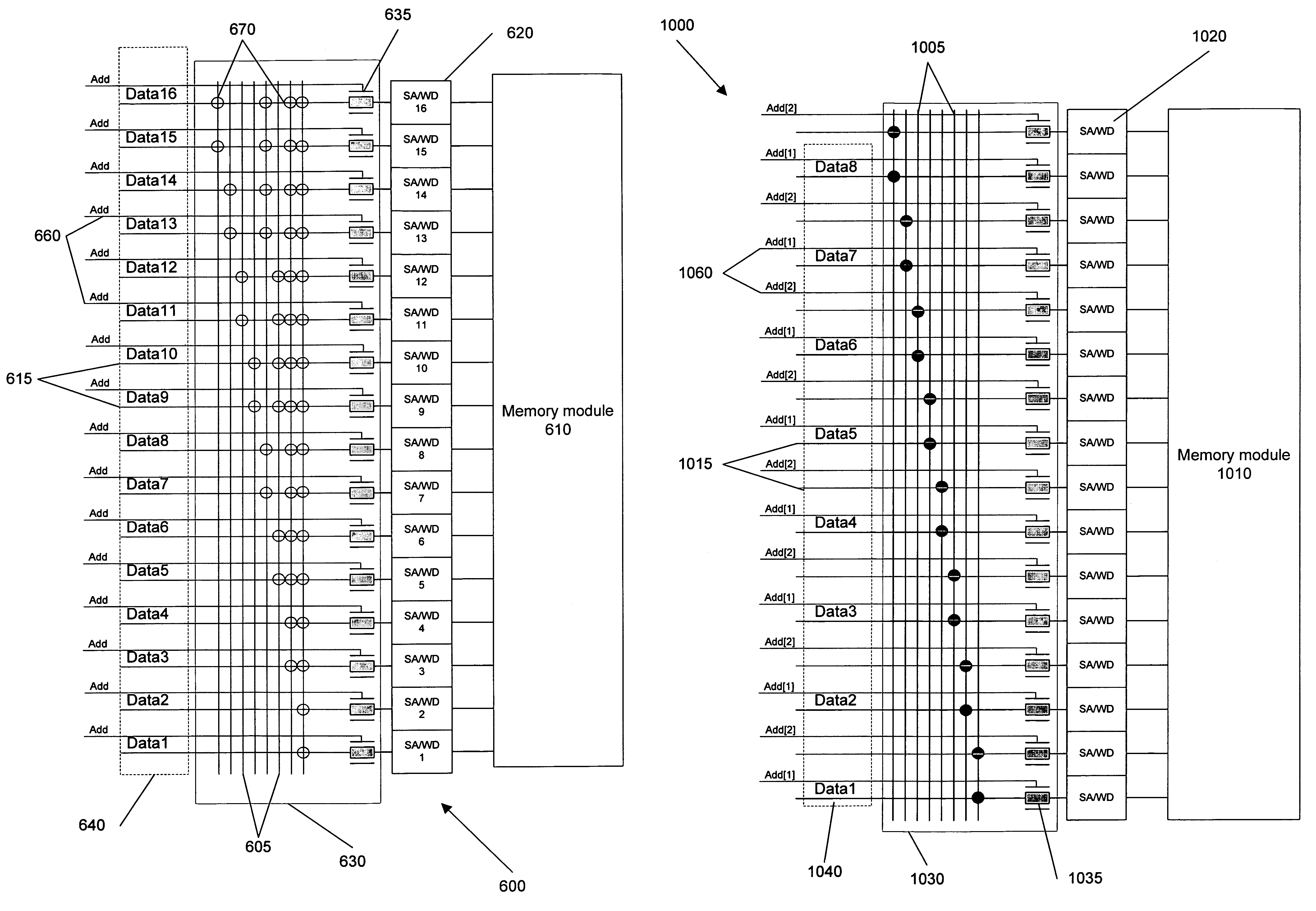
[0022]FIG. 1 shows an I / O device 100 with a memory module 110 capable of transferring data up to sixteen bits (X16) at a time. Each bit is transmitted through one of sixteen sense amplifier / write drivers (SA / WD) 120. During an operation of reading data from the memory module 110, each SA / WD may load in a different bit of data from the memory module 110. The data bits are then transmitted to a muxing structure (or memory interface) 130 f...


PUM


Abstract

The present invention provide circuits, methods, and apparatus directed to an integrated circuit having a memory interface that is configurable to have one of a multiple different bus widths. The memory interface has a first set of lines and a second set of lines. The first and second set of lines are arranged such that there are multiple locations at which a via may be placed to connect a line of the first set to a line of the second set. The placement of the vias determines the bus width of the memory interface.

Description

BACKGROUND OF THE INVENTION[0001]This invention relates to switching or multiplexing structures for sending and retrieving variable amounts of data from memory or other circuit elements within integrated circuit devices. Devices of the type that are sometimes known as structured application-specific integrated circuits (“structured ASICs”) may particularly benefit.[0002]A possible use of structured ASIC technology is to produce ASICs that are functionally equivalent to programmed field-programmable gate arrays (“FPGAs”). After a logic design has been adequately “proven” in an FPGA, the design may be “migrated” to a structured ASIC. Structured ASICs offer several key performance advantages over FPGAs, primarily in the areas of power reduction, clock performance, manufacturing costs, and core density. A potential competing concern that might reduce such benefits of the migration from an FPGA to an ASIC is maintaining equivalent functionality between the ASIC and the FPGA.[0003]For ins...

Claims


Application Information

Patent Timeline
Patent Type & Authority Patents(United States)
IPC IPC(8): G11C5/06
CPCG11C5/063G11C7/1006G11C7/1051
Inventor CHOE, KOK HENG
Owner ALTERA CORP
Why Eureka
Try Eureka