Integrated circuit comprising an array of single photon avalanche diodes

a technology of integrated circuits and diodes, which is applied in the field of integrated circuits comprising single photon avalanche diodes, can solve the problems of incompatibility of sensors, spads cannot store brightness information, and existing arrays of spads suffer from limited lateral resolution, so as to achieve high performance and reduce power consumption

Active Publication Date: 2009-06-16
FASTREE 3D SA
View PDF32 Cites 81 Cited by
  • Summary
  • Abstract
  • Description
  • Claims
  • Application Information

AI Technical Summary

Benefits of technology

[0015]This has the advantage that, among others, at least part of the read-out circuits are shared between several pixels, thus reducing the number of transistors per pixels and improving the fill-in factor of the circuit. Furthermore, the number of power-hungry read-out circuits is reduced.
[0016]At least some part of the read-out circuit, such as the counters and TDCs, can be moved outside the SPAD array, but preferably on the same chip. This has the advantage that the fill-in factor of the SPAD array can be improved, thus the distance between pixels reduced.
[0017]Several SPADs, for example all SPADs in a row, can be read simultaneously and the corresponding digital values stored in a memory store on the chip. The next rows will be read at a different time and the corresponding values stored in the same memory store, at the same address or at a different location. The memory store is preferably on the same chip, but outside the SPAD array. Thus, communications required for the outside world are reduced by processing information on-chip and by multiplexing information on few data and address lines.
[0020]The present invention thus proposes a new pixel readout circuit which is shared between a group of pixels, e.g. all the pixels in a same column or row. The disclosed circuit is capable of handling simultaneously all the concerned pixels so that pixel size can be reduced and fill factor can be significantly improved. The proposed readout circuit architecture is capable of handling simultaneously a cluster of several pixels almost in parallel so that partial counts at pixel-level do not need to be stored.
[0022]This has the advantage of coupling the SPAD with the read-out circuit using galvanic isolation techniques while maintaining high performance and reducing power consumption. Furthermore, the proposed method is very useful in mainstream semiconductor technologies such as standard CMOS and / or BiCMOS processes.

Problems solved by technology

Existing arrays of SPADs suffer from a limited lateral resolution due to the lack of an efficient readout circuitry.
Indeed SPADs cannot store brightness information since single photon detection is translated to a discrete electrical pulse.
The sensor is not CMOS compatible and necessitates a complex technology which is expensive and hard to integrate on a monolithic integrated circuit.
Use of two different chips and wire-bonding of the chips, makes the fabrication of very high resolution chip expensive.
Multiple technologies could be combined into a single chip; however this is also an expensive proposition.
The process unfortunately uses a more expensive and non-standard CMOS technology.
Furthermore, high-voltage transistors, which require more power, are additionally area-expensive devices which lead to an extremely low fill-factor if an array of SPADs were to be implemented.
This solution is thus hardly scalable, and poorly adapted to arrays comprising tens or even hundreds of SPADs, as required by modern imagers.
This behavior limits the photo-detection for red and infrared photons, which are absorbed more deeply in the substrate.
Unfortunately, in the n-well, minor carriers are holes which mobility and ionization coefficient are much lower than those of electrons.
This further reduces the photo-detection capability of such SPADs based on that method.

Method used


Image

  • Integrated circuit comprising an array of single photon avalanche diodes
  • Integrated circuit comprising an array of single photon avalanche diodes
  • Integrated circuit comprising an array of single photon avalanche diodes

Examples


Embodiment Construction

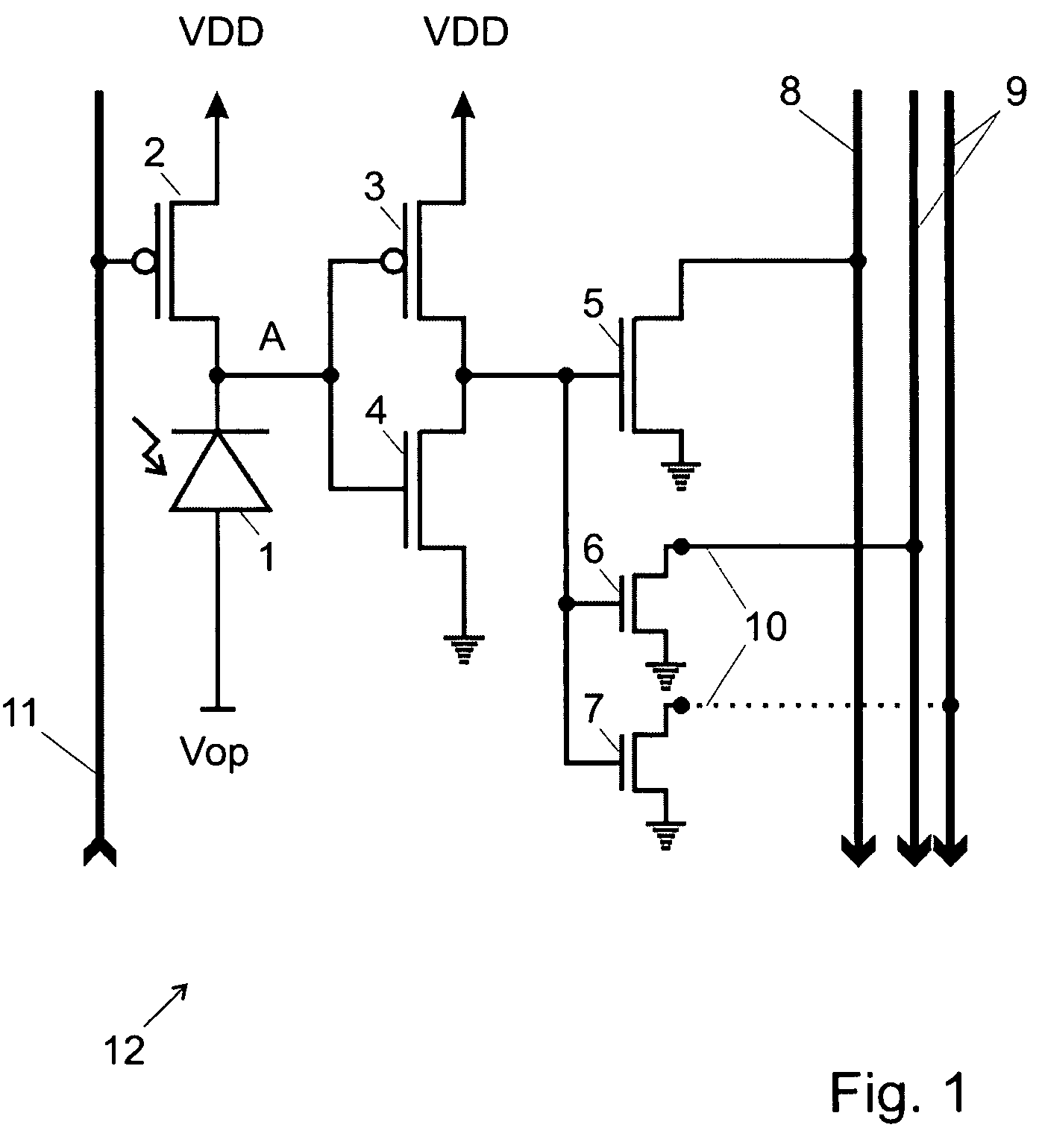
[0028]FIG. 1 shows an embodiment of a pixel 12 based on a SPAD (single photon avalanche diode). A SPAD is a p-n junction biased above breakdown voltage Vbd by an excess voltage Ve of a few volts. Operated in the so-called Geiger mode, avalanche photodiodes can react on single photons. A primary carrier resulting from the absorption of a photon may generate a nearly-infinite number of secondary electron-hole pairs by impact ionization.

[0029]In the embodiment of pixel illustrated by FIG. 1, reference numeral 1 represents the SPAD; 2 is a quenching (recharging) transistor; 3 and 4 define a CMOS inverter, 5 is the output transistor, 6 and 7 represent addressing transistors, 8 is a shared output bus line, 9 denotes shared address bus lines, 10 are connections used to code the pixel address, 11 is an optional recharging line.

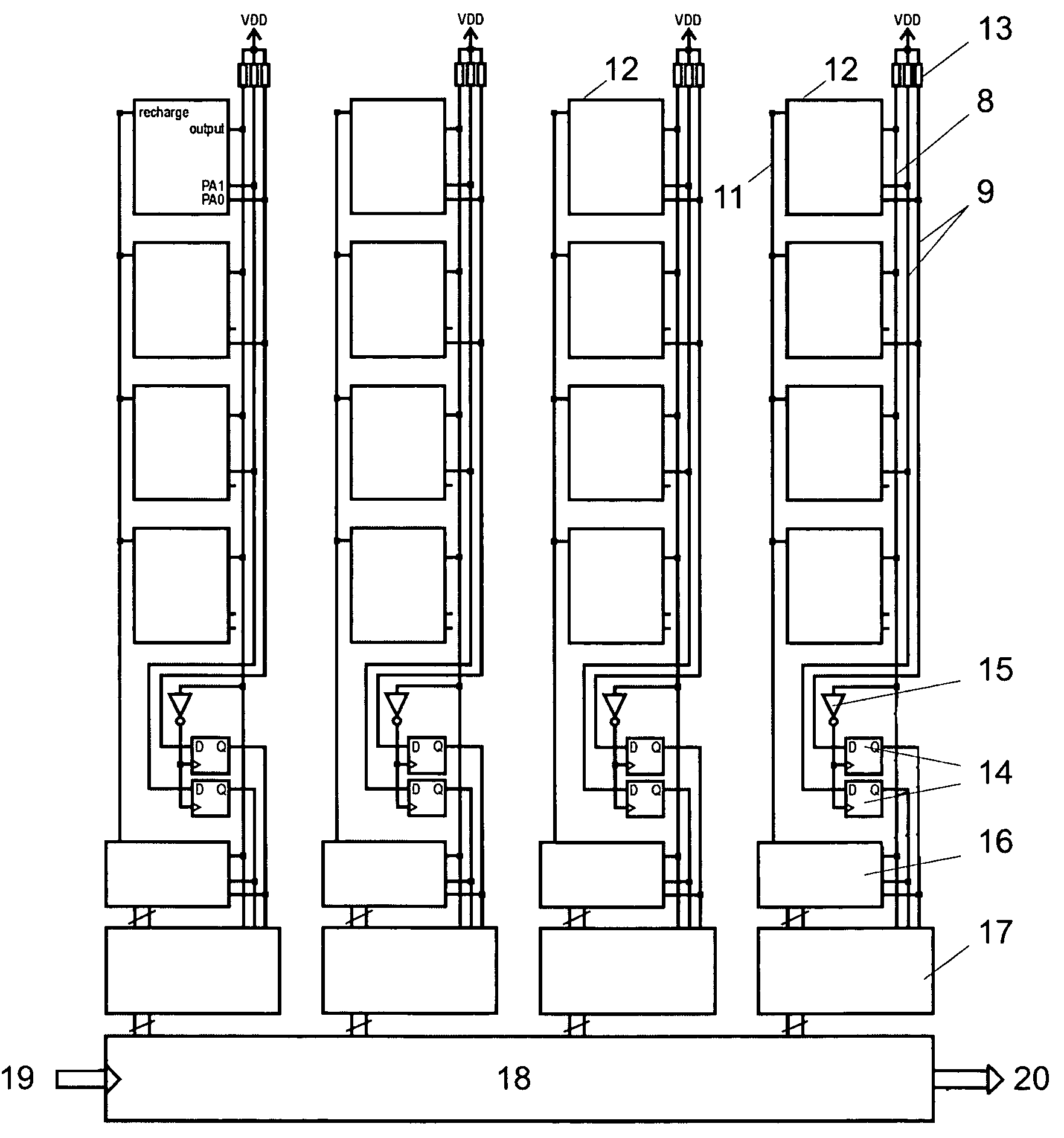
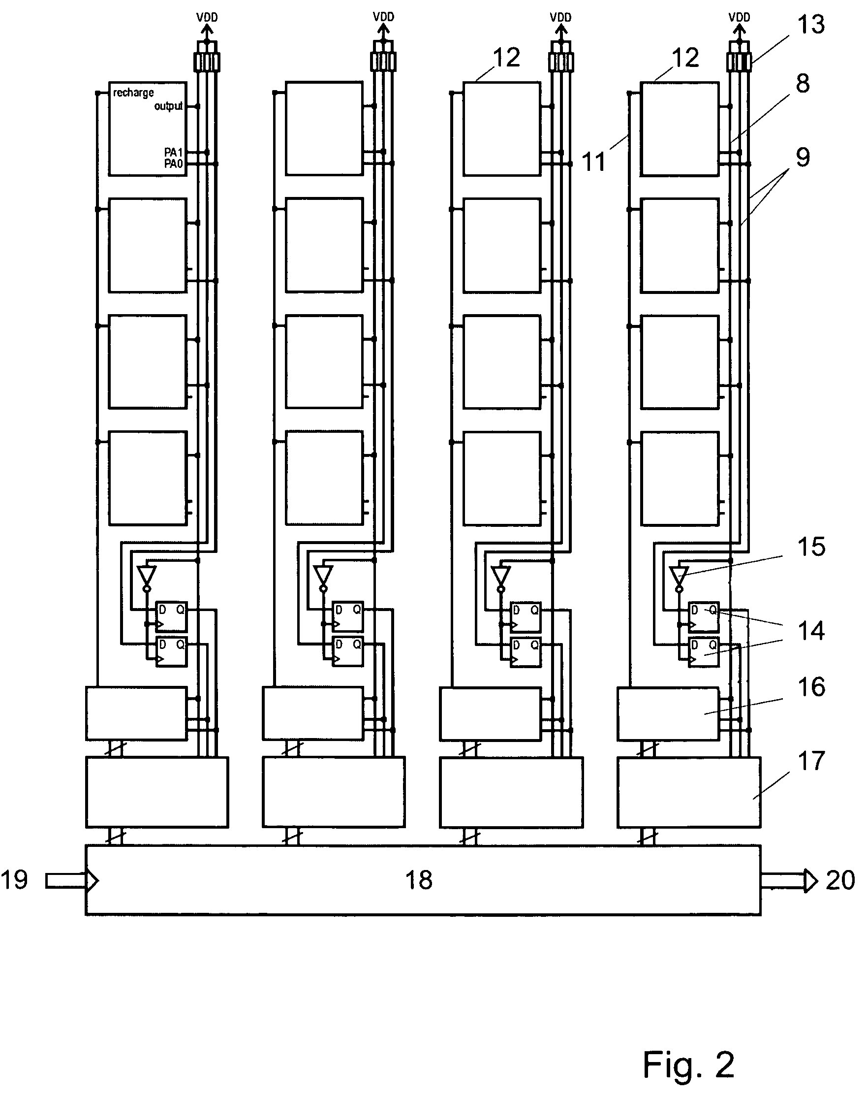
[0030]FIG. 2 shows an example of the proposed architecture whereby the pixel readout circuit is arranged in columns. In order to simplify the description, a m×n array...


PUM


Abstract

An integrated circuit (1) has an array of single photon avalanche diodes (SPADS), a plurality of read-out circuits, each SPADS being coupled to one read-out circuit, wherein at least some of the read-out circuits comprise time-to-digital converters (TDC) and / or a digital asynchronous counter. The plurality of SPADS are coupled to one single read-out circuit. The read-out circuit may have a transformer for decoupling the SPAD from other parts of the read-out circuit.

Description

[0001]The present application also incorporates by reference the content of U.S. utility patent application U.S. Ser. No. 11 / 290,831, filed on Dec. 1, 2005, and of U.S. provisional patent application U.S. 60 / 652,010, filed on Feb. 14, 2005.[0002]The present application claims priority of EP patent application 2005EP-101069 (EP05101069.2), filed on Feb. 14, 2005.FIELD OF THE INVENTION[0003]The present invention concerns a circuit comprising at least one single photon avalanche diodes (SPADs), or an array of such SPADs. The present invention concerns in particular electronic read-out circuits for processing electrical pulses generated by said SPADs. The present invention also relates to new applications for SPADs and SPAD arrays.DESCRIPTION OF RELATED ART[0004]Single photon avalanche diodes (SPADs) are photodiodes operating in the so-called Geiger mode. SPADs have several advantages over photodiodes operating in the linear mode. Among the most important ones are a higher sensitivity a...

Claims


Application Information

Patent Timeline
Patent Type & Authority Patents(United States)
IPC IPC(8): H01J40/14H01L27/00H04N3/14
CPCG01T1/248G01S17/10G01S17/894G01S7/4863
Inventor NICLASS, CRISTIANOCHARBON, EDOARDO
Owner FASTREE 3D SA
Why Eureka
Try Eureka