High-speed, low-power level shifter for mixed signal-level environments

a level shifter, low-power technology, applied in logic circuits, pulse automatic control, pulse techniques, etc., can solve the problems of reducing affecting the switching speed of the signal level shifter, and requiring the added expense of a dual oxide process, so as to achieve fast switching times

Inactive Publication Date: 2009-06-30
INTEGRATED DEVICE TECH INC
View PDF19 Cites 19 Cited by
  • Summary
  • Abstract
  • Description
  • Claims
  • Application Information

AI Technical Summary

Benefits of technology

[0007]In accordance with some embodiments of the present invention, a level shifter is presented that allows for fast switching times. In some embodiments, the level shifter is protected from over voltage situations that can damage the thin gate oxide material.

Problems solved by technology

These later reductions to one volt supply designs now require the added expense of a dual oxide process, for example an 80 Å process for device potentials of 3.3 volts and a 16 Å process for device potentials of 1.0 volts.
The lower device potentials can result in lower power consumption.
Application of voltages greater than the design specification for a particular gate oxide thickness can result in damage to the transistor.
Further, application of high voltage power supplies in circuits that are formed with lower voltage transistors can affect the timing of those circuits.

Method used


Image

  • High-speed, low-power level shifter for mixed signal-level environments
  • High-speed, low-power level shifter for mixed signal-level environments
  • High-speed, low-power level shifter for mixed signal-level environments

Examples


Embodiment Construction

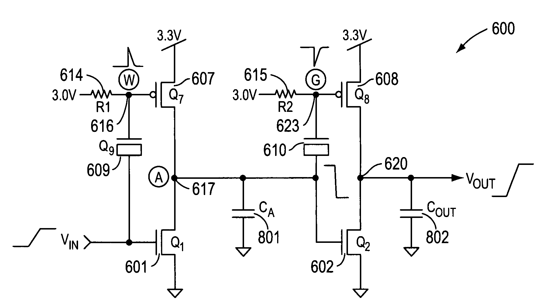
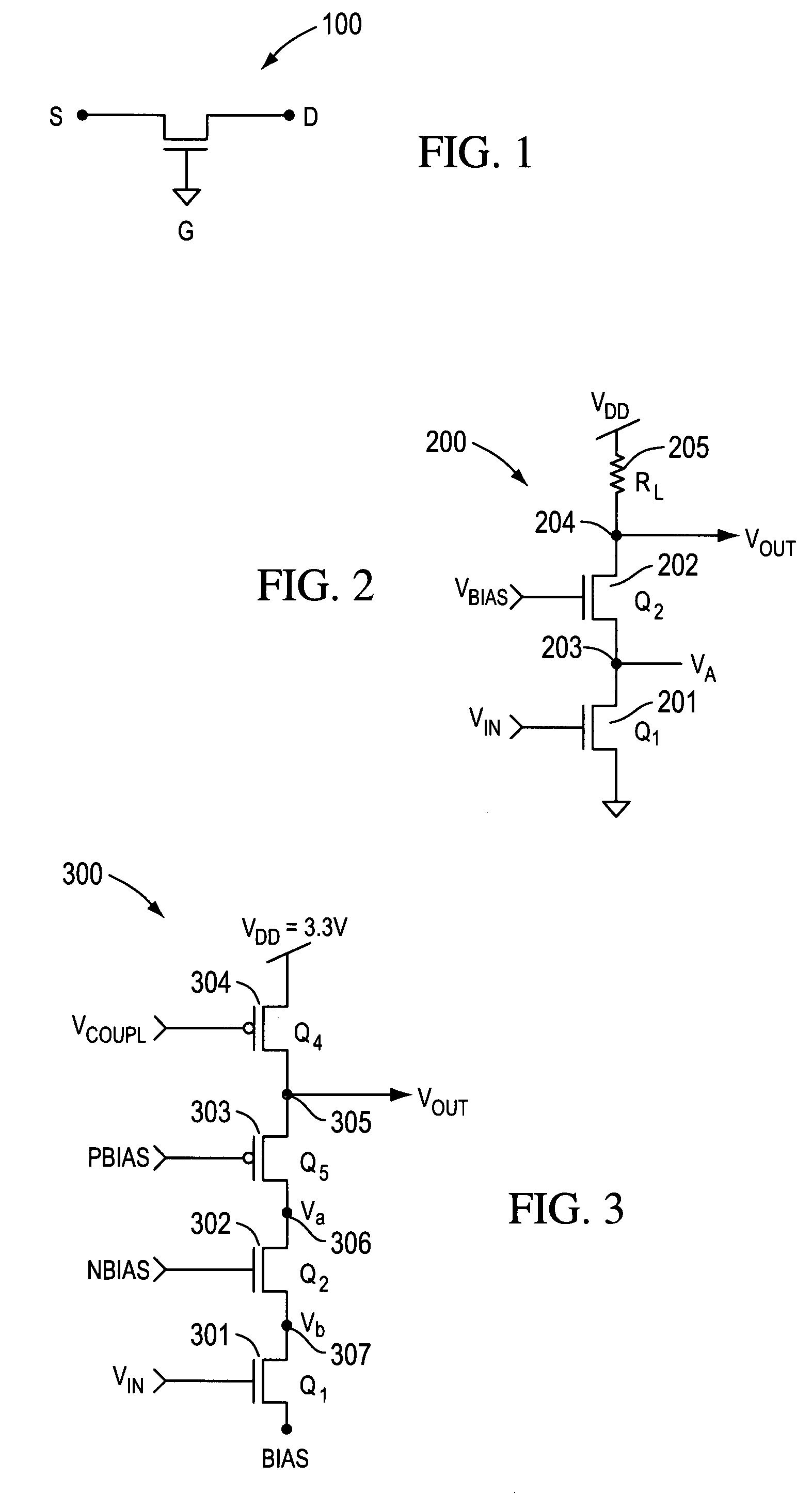
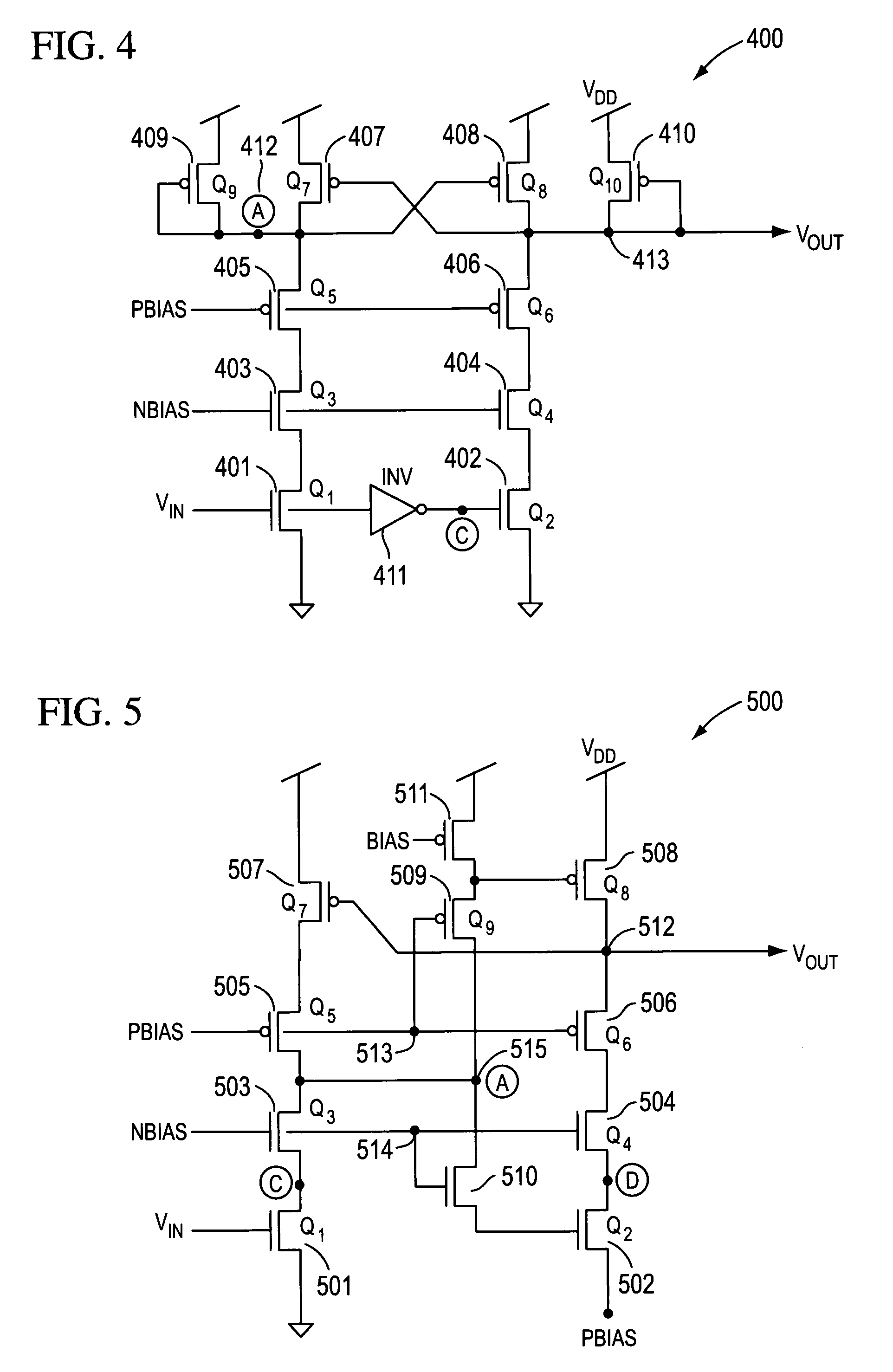
[0027]In accordance with some embodiments of the present invention, a circuit that converts a low voltage signal to a high voltage signal with a swing that does not damage the thin gate oxides is presented. Conventional circuits that perform this task have characteristic delays of nanoseconds and power dissipation of milliwatts. Some circuits according to the present invention have delays measured in picoseconds and power dissipation measured in microwatts.

[0028]In accordance with some embodiments of the present invention, a two stage level shifting circuit includes p-channel and n-channel transistors biased so as to limit the potential drops between the source gate and between the gate and drain of the series p-channel transistor, and the voltage potential drops between the drain and gate and between the gate and source of the n-channel transistors to within the reliability limits of the transistors. The source nodes of pull-down n-channel transistors of both stages are source bias...


PUM


Abstract

A level shifter is presented that allows fast switching while requiring low power. In accordance with some embodiments of the invention, the level shifter is a two stage level shifting circuit with p-channel and n-channel transistors biased so as to limit the potential between the source to gate or drain to gate of any of the transistors. Pull-up transistors are placed in a transition state so that spikes resulting from an increasing or decreasing input voltage turn on or off the pull up transistors to assist in the switching.

Description

BACKGROUND[0001]1. Field of the Invention[0002]The present invention is related to a level shifter and, in particular, to a high-performance level shifter for use with thin gate-oxide devices.[0003]2. Discussion of Related Art[0004]Circuit development is often a result of technological change. In the 1960's the N-channel MOS gate oxide thicknesses were about 2000 Å in order to support gate bias potentials of about 18 volts. In the last ten years, products that were designed with 130 Å thick gates for five volt supplies are now designed for operating supply voltages of 3.3 volts with core supplies of 2.5 volts. More recent designs with core voltages of 1.0 volts have 3.3 volt external drives with gate oxides of core transistors of 16 Å gate thicknesses. These later reductions to one volt supply designs now require the added expense of a dual oxide process, for example an 80 Å process for device potentials of 3.3 volts and a 16 Å process for device potentials of 1.0 volts. The lower d...

Claims


Application Information

Patent Timeline
Patent Type & Authority Patents(United States)
IPC IPC(8): H03L5/00
CPCH03K19/0013H03K19/01707H03K19/018521
Inventor PILLING, DAVID J.AU, MARIO FULAM
Owner INTEGRATED DEVICE TECH INC
Why Eureka
Try Eureka