

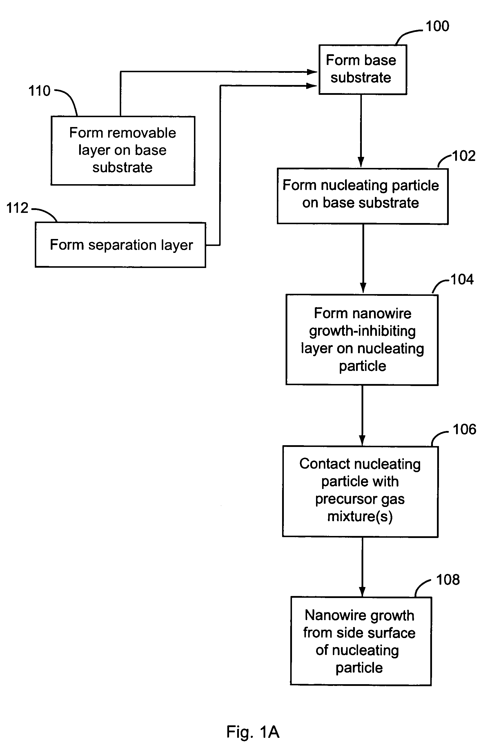
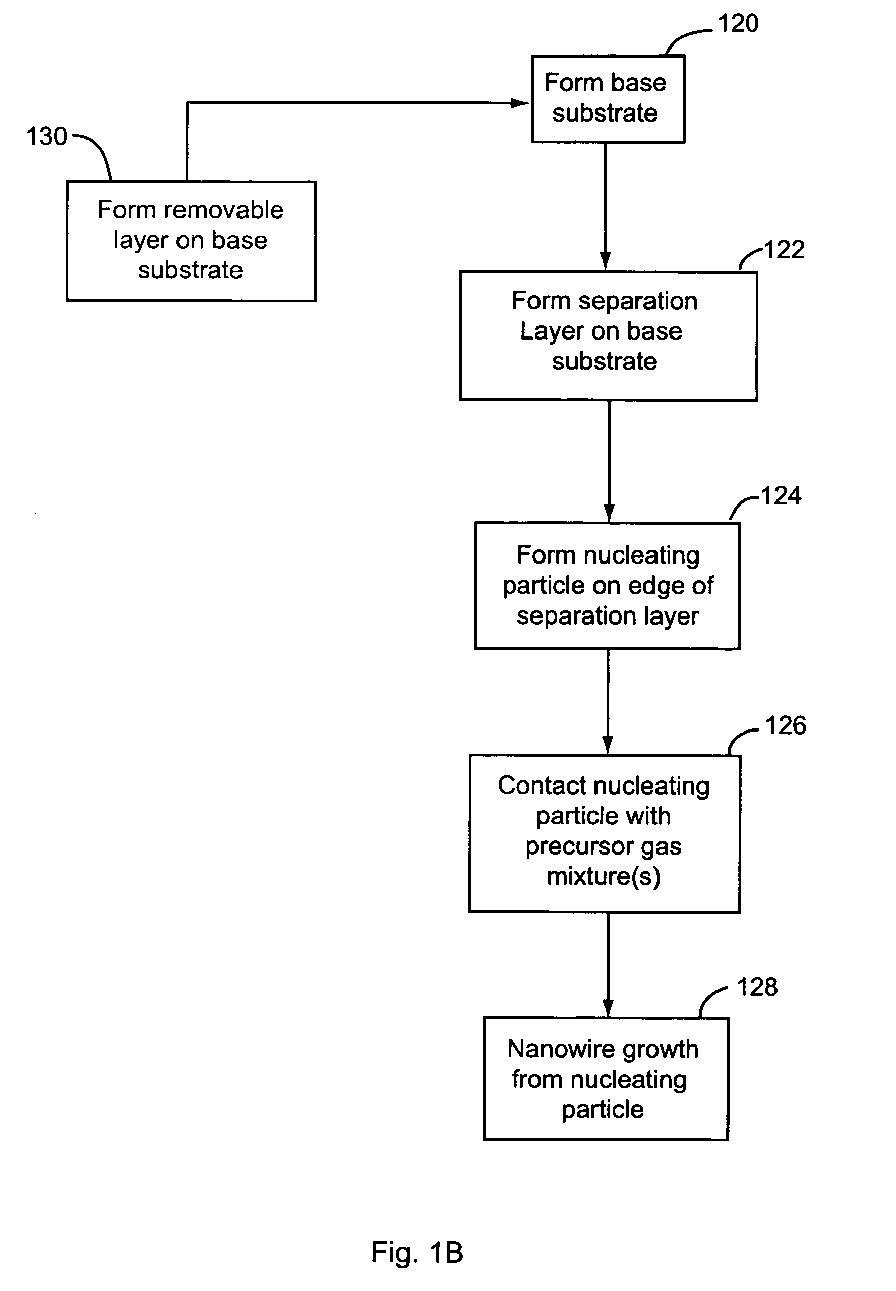
Nanowire horizontal growth and substrate removal
a technology of nanowires and substrates, applied in the direction of crystal growth process, polycrystalline material growth, chemistry apparatus and processes, etc., can solve the problems of difficult integration of nanowires for creating devices, amorphous silicon and organic semiconductors have performance limitations, and require relatively expensive processing, etc., to achieve easy transfer, processing and/or harvesting
- Summary
- Abstract
- Description
- Claims
- Application Information
AI Technical Summary
Benefits of technology
Problems solved by technology
Method used
Image

Examples
Embodiment Construction
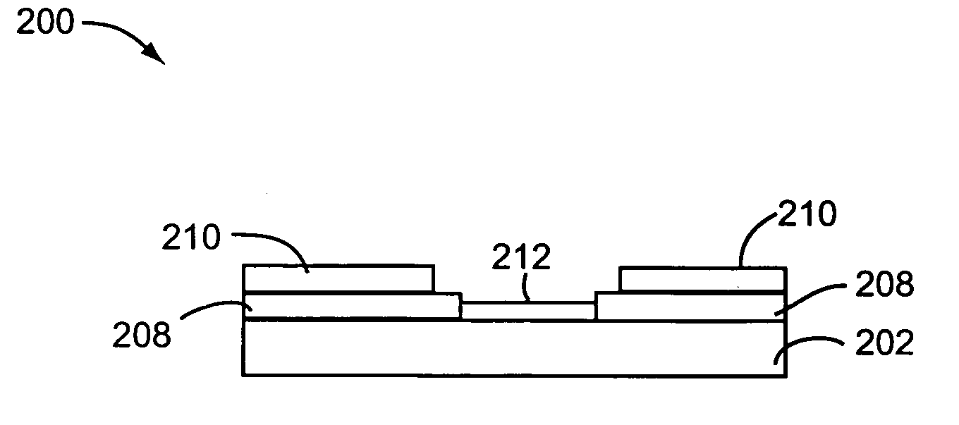
[0029]The growth of wires from the side walls of a trench (horizontally) is similar to wire growth on a surface (vertically) as both rely on growth out of the surface of a film (thickness defines drop size and hence wire diameter) or colloidal particles placed on the side wall of the trench. The processes of the present invention are advantageous because they produce horizontal, substantially separate, oriented, nanowires that do not require the removal of the wires from the growth substrate after growth for post-processing of the wires, and limit the need for unconventional processing techniques during device manufacturing.
[0030]It should be appreciated that the particular implementations shown and described herein are examples of the invention and are not intended to otherwise limit the scope of the present invention in any way. Indeed, for the sake of brevity, conventional electronics, manufacturing, semiconductor devices, and nanowire (NW), nanorod, nanotube, and nanoribbon tech...
PUM
| Property | Measurement | Unit |
|---|---|---|
| carrier mobility | aaaaa | aaaaa |
| thickness | aaaaa | aaaaa |
| aspect ratio | aaaaa | aaaaa |
Abstract
Description
Claims
Application Information