Memory cell sidewall contacting side electrode

a memory cell and side electrode technology, applied in semiconductor devices, digital storage, instruments, etc., can solve the problems of poor and achieve the effect of poor resulting strength of the top interfa

Active Publication Date: 2009-08-04
MACRONIX INT CO LTD
View PDF324 Cites 54 Cited by
  • Summary
  • Abstract
  • Description
  • Claims
  • Application Information

AI Technical Summary

Benefits of technology

[0011]Conventional memory cells of the type including a memory material switchable between electrical property states by the application of energy, in particular phase change random access memory devices, typically have the side electrode deposited onto the surface of the phase change material. The resulting strength of the top interface is often poor because the coefficient of thermal expansion of the typical phase change material, such as GST, is larger than the coefficient of thermal expansion of the typical side electrode material, such as TiN. This contrasts with the interface between the phase change material and a bottom electrode because the phase change material is deposited onto the bottom electrode. The present invention helps to eliminate this weak top interface problem because the memory material is deposited onto both the bottom electrode and the side electrode.

Problems solved by technology

The resulting strength of the top interface is often poor because the coefficient of thermal expansion of the typical phase change material, such as GST, is larger than the coefficient of thermal expansion of the typical side electrode material, such as TiN.

Method used


Image

  • Memory cell sidewall contacting side electrode
  • Memory cell sidewall contacting side electrode
  • Memory cell sidewall contacting side electrode

Examples


Embodiment Construction

[0021]The following description of the invention will typically be with reference to specific structural embodiments and methods. It is to be understood that there is no intention to limit the invention to the specifically disclosed embodiments and methods but that the invention may be practiced using other features, elements, methods and embodiments. Preferred embodiments are described to illustrate the present invention, not to limit its scope, which is defined by the claims. Those of ordinary skill in the art will recognize a variety of equivalent variations on the description that follows. Like elements in various embodiments are commonly referred to with like reference numerals.

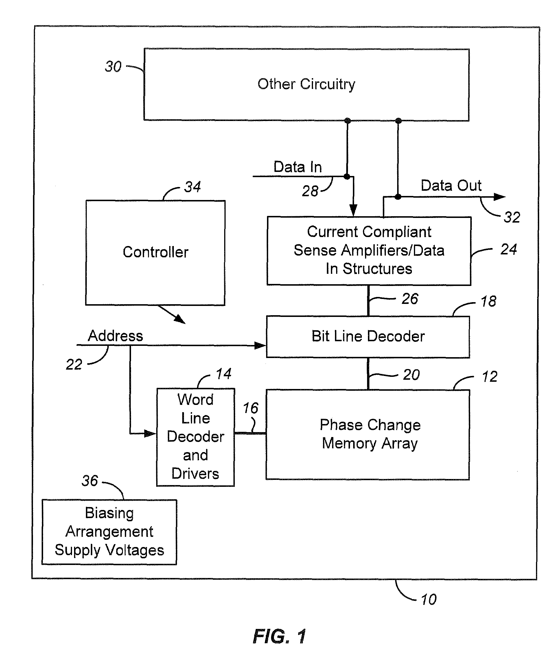
[0022]Referring to FIG. 1, shown is a simplified block diagram of an integrated circuit 10 in which the present invention may be implemented. Circuit 10 includes a memory array 12 implemented using phase change memory cells (not shown) on a semiconductor substrate, discussed more fully below. A word line...


PUM


Abstract

A memory cell includes a memory cell layer over a memory cell access layer. The memory cell access layer comprises a bottom electrode. The memory cell layer comprises a dielectric layer and a side electrode at least partially defining a void with a memory element therein. The memory element comprises a memory material switchable between electrical property states by the application of energy. The memory element is in electrical contact with the side electrode and with the bottom electrode. In some examples the memory element has a pillar shape with a generally constant lateral dimension with the side electrode and the dielectric layer surrounding and in contact with first and second portions of the memory element.

Description

BACKGROUND OF THE INVENTION[0001]1. Field of the Invention[0002]The present invention relates to high density memory devices based on memory materials, for example resistor random access memory (RRAM) devices, and to methods for manufacturing such devices. The memory material is switchable between electrical property states by the application of energy. The memory materials may be phase change based memory materials, including chalcogenide based materials, and other materials.[0003]2. Description of Related Art[0004]Phase change based memory materials are widely used in read-write optical disks. These materials have at least two solid phases, including for example a generally amorphous solid phase and a generally crystalline solid phase. Laser pulses are used in read-write optical disks to switch between phases and to read the optical properties of the material after the phase change.[0005]Phase change based memory materials, like chalcogenide based materials and similar materials, ...

Claims


Application Information

Patent Timeline
Patent Type & Authority Patents(United States)
IPC IPC(8): H01L29/02G11C11/56H01L21/00
CPCH01L45/06H01L45/1253H01L45/144H01L45/122H01L45/1683H01L27/2436H01L27/2463H01L45/1625Y10S438/90H10B63/30H10B63/80H10N70/821H10N70/231H10N70/841H10N70/8828H10N70/026H10N70/066
Inventor LUNG, HSIANG-LAN
Owner MACRONIX INT CO LTD
Why Eureka
Try Eureka