Circuit board and process for manufacturing the same

Inactive Publication Date: 2011-06-30
UNIMICRON TECH CORP
View PDF10 Cites 3 Cited by
  • Summary
  • Abstract
  • Description
  • Claims
  • Application Information

AI Technical Summary

Benefits of technology

[0008]The present invention provides a circuit board and a process for manufactu

Problems solved by technology

Since the depth of the blind via is different from the depth of the intaglio, the electroplating condition is not easy to be controlled when the electroplating process is performed, which leads to poor uniformity of the thickness of the conductive layer.
Therefore, when a process for removing a portion of the conductive layer at the outside of the intaglio and the blind via is later performed, it is hard to control the thickness of the removed portion of the conductive layer.
Hence,

Method used


Image

  • Circuit board and process for manufacturing the same
  • Circuit board and process for manufacturing the same
  • Circuit board and process for manufacturing the same

Examples


Example

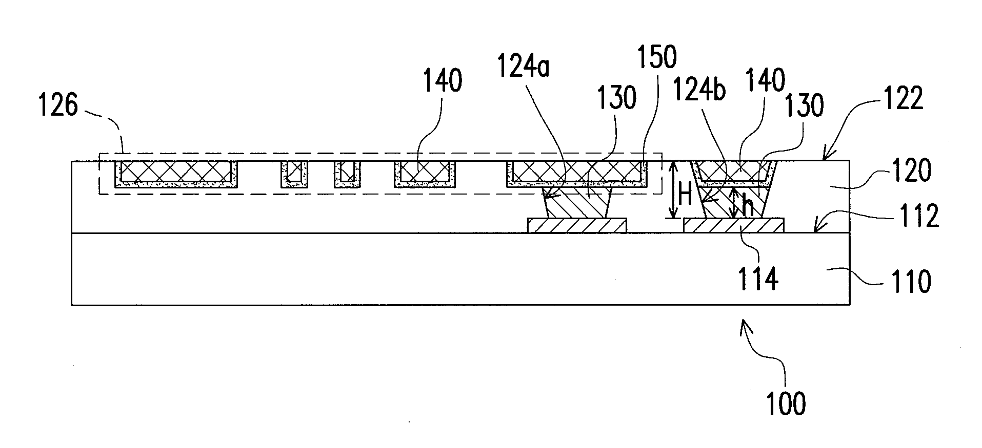
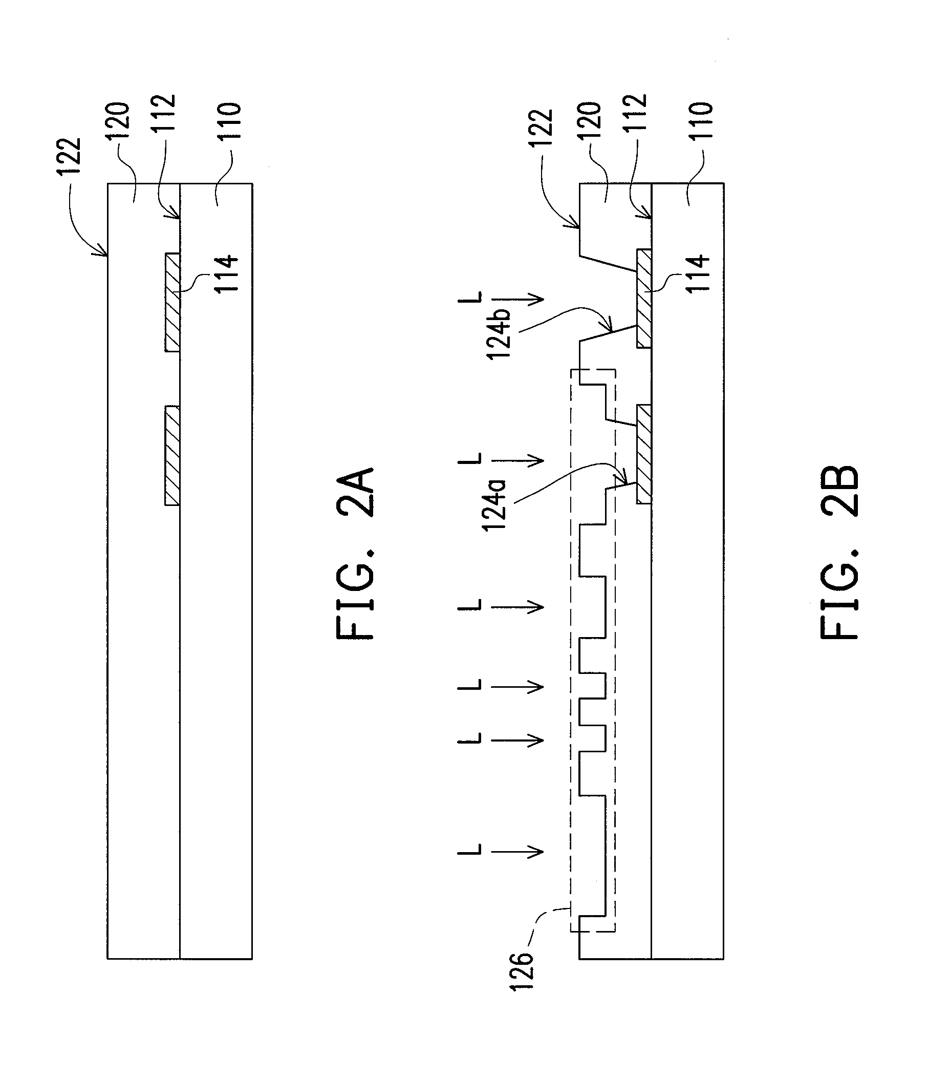
[0031]FIG. 1 is a schematic cross-sectional view of a circuit board according to one embodiment of the present invention showing. Referring to FIG. 1, in the present embodiment, a circuit board 100 includes a circuit substrate 110, a dielectric layer 120, a first conductive layer 130 and a second conductive layer 140. It should be noticed that the structure of the circuit board 100 can have a single-layered circuit layer or a multi-layered circuit layer. That is, the circuit board 100 can be a single-layered circuit board, a double-layered circuit board or a multi-layered circuit board. In the present embodiment, the circuit board 100 depicted in FIG. 1 as a build-up wiring board is used to describe the invention.

[0032]Specifically, the circuit substrate 110 has a first surface 112 and a first circuit layer 114, wherein the first circuit layer 114 is disposed on the first surface 112 of the circuit substrate 110. That is to say, the first circuit layer 114 can be a kind of normal ci...


PUM

PropertyMeasurementUnit
Electrical conductanceaaaaaaaaaa
Electrical conductoraaaaaaaaaa

Abstract

A circuit board including a circuit substrate, a dielectric layer, a first conductive layer and a second conductive layer is provided. The circuit substrate has a first surface and a first circuit layer. The dielectric layer is disposed on the circuit substrate and covers the first surface and the first circuit layer. The dielectric layer has a second surface, at least a blind via extended from the second surface to the first circuit layer and an intaglio pattern. The first conductive layer is disposed inside the blind via. The second conductive layer is disposed in the intaglio pattern and the blind via and covers the first conductive layer. The second conductive layer is electrically connected with the first circuit layer through the first conductive layer.

Description

CROSS-REFERENCE TO RELATED APPLICATION[0001]This application claims the priority benefit of Taiwan application serial no. 98145798, filed on Dec. 30, 2009. The entirety of the above-mentioned patent application is hereby incorporated by reference herein and made a part of this specification.BACKGROUND OF THE INVENTION[0002]1. Field of the Invention[0003]The present invention relates to a circuit board and a process for manufacturing the same. More particularly, the present invention relates to a circuit board with a relatively better reliability and a process for manufacturing the circuit board.[0004]2. Description of Related Art[0005]According to the current technologies, an embedded circuit board has been evolved from a common non-embedded circuit board. In particular, the common non-embedded circuit board is characterized in that circuits therein protrude from a surface of a dielectric layer. By contrast, circuits of the embedded circuit board are buried in the dielectric layer. ...

Claims


Application Information

Patent Timeline
IPC IPC(8): H05K1/11H05K3/00
CPCH05K2201/0376Y10T29/49165Y10T29/49126H05K3/421Y10T29/49117H05K2203/1476Y10T29/49155H05K1/115H05K3/107H05K1/0298
Inventor TSENG, TZYY-JANGCHIANG, SHU-SHENGCHEN, TSUNG-YUAN
Owner UNIMICRON TECH CORP
Why Eureka
Try Eureka