Power amplifier

a power amplifier and amplifier technology, applied in the direction of amplifiers, amplifiers with semiconductor devices only, amplifiers with semiconductor devices, etc., to achieve the effect of less power and smaller chip area

Inactive Publication Date: 2009-08-18
PANASONIC SEMICON SOLUTIONS CO LTD
View PDF8 Cites 8 Cited by
  • Summary
  • Abstract
  • Description
  • Claims
  • Application Information

AI Technical Summary

Benefits of technology

[0011]With the foregoing in mind, it is an object of the present invention to provide a small and low power-consuming amplifier that can be driven with a low power supply voltage, and in which deterioration in efficiency or linearity of the amplifier can be prevented.
[0014]According to the present invention, a power amplifier is improved so that a current variation resulting from a variation in hFE is suppressed, so as to be driven with a low supply power voltage. Accordingly, a power amplifier consuming less power and requiring a smaller chip area can be obtained.
[0015]Further, according to the power amplifier having the second configuration, an inflow of an RF signal to the current reference transistor can be prevented.

Problems solved by technology

Hence, when a general SiGe process is considered, a power supply voltage of at least 1.6 V is needed since the voltage between the emitter and the base is about 0.8 V. This is inconvenient when a variation in power supply voltage and various kinds of dispersions are taken into consideration.

Method used


Image

  • Power amplifier
  • Power amplifier
  • Power amplifier

Examples


embodiment 1

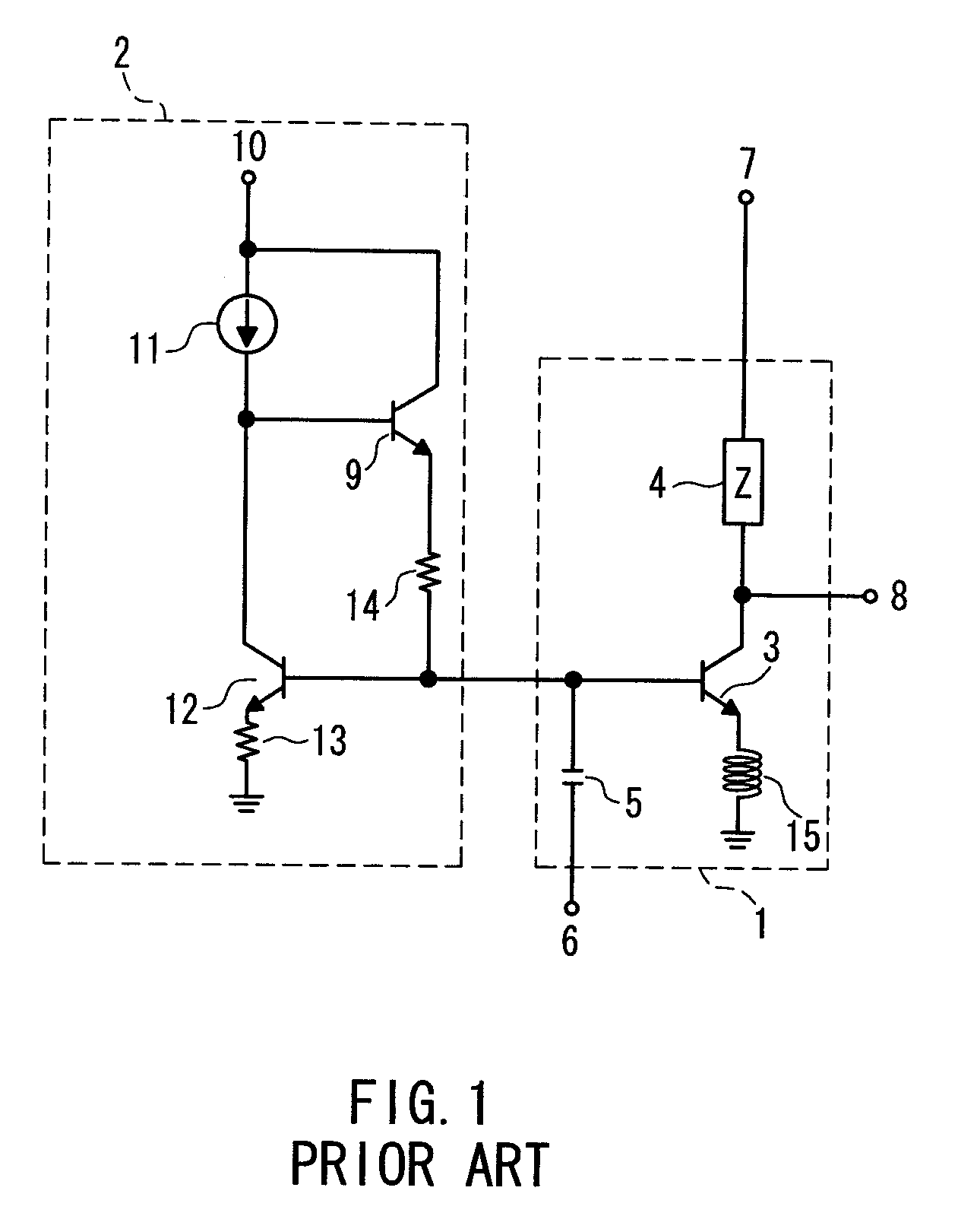
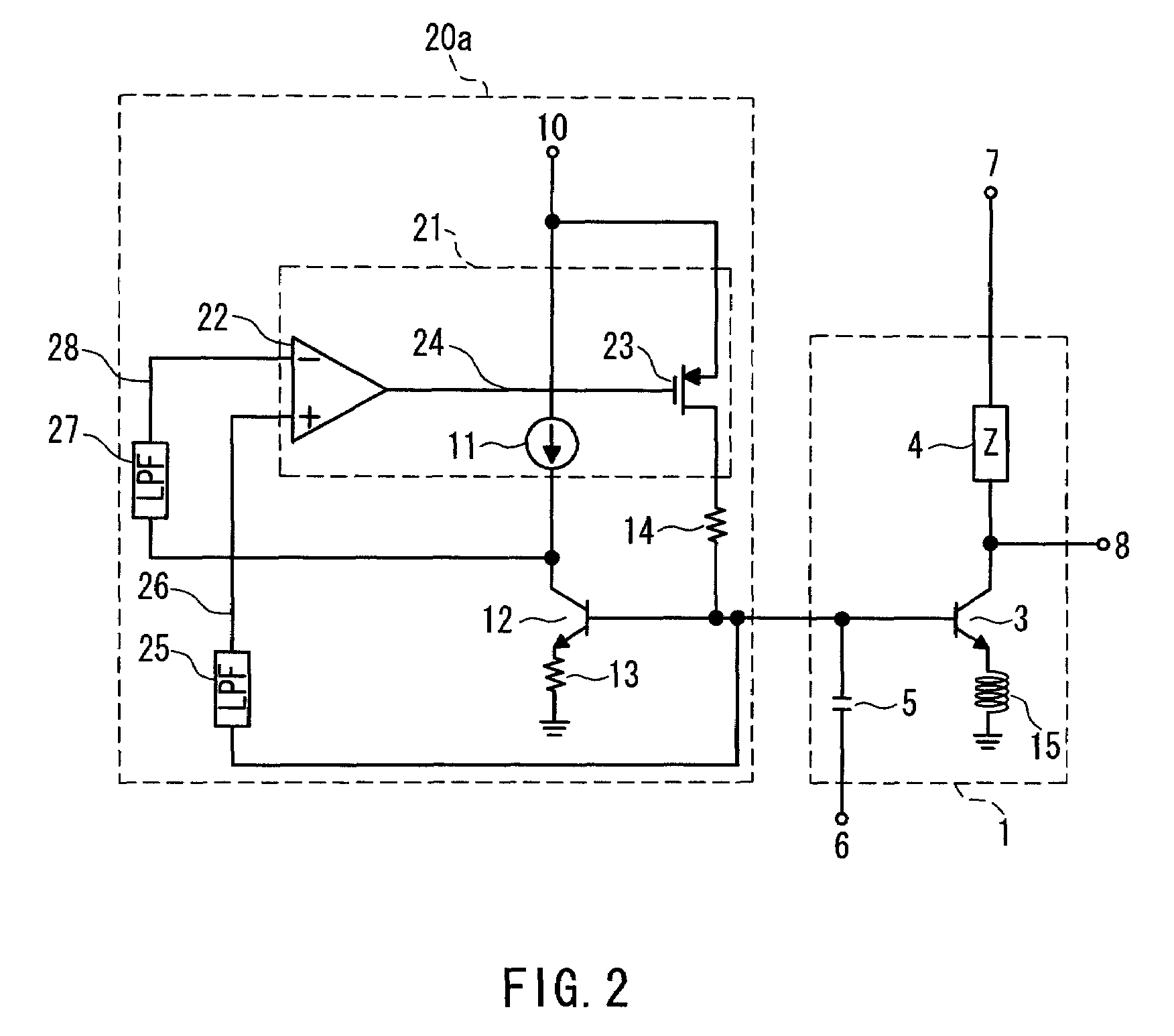
[0033]FIG. 2 is a circuit diagram showing a power amplifier according to a first embodiment of the present invention. This power amplifier includes the RF operation section 1 and a DC bias circuit 20a. Similarly to the RF operation section 1 in the conventional example shown in FIG. 1, the RF operation section 1 includes the RF operation transistor 3, the impedance 4, the DC blocking capacitor 5, and the feedback inductor 15. Accordingly, redundant description will be omitted.

[0034]The DC bias circuit 20a has a configuration in which the base current compensation transistor 9 in the DC bias circuit 2 shown in FIG. 1 is replaced by a base current compensation circuit 21. Therefore, the same reference numerals will be assigned to the identical elements, and redundant description will be omitted. The base current compensation circuit 21 includes an operational amplifier 22 formed of CMOS and a voltage-to-current conversion transistor 23. An output 24 of the operational amplifier 22 is ...

embodiment 2

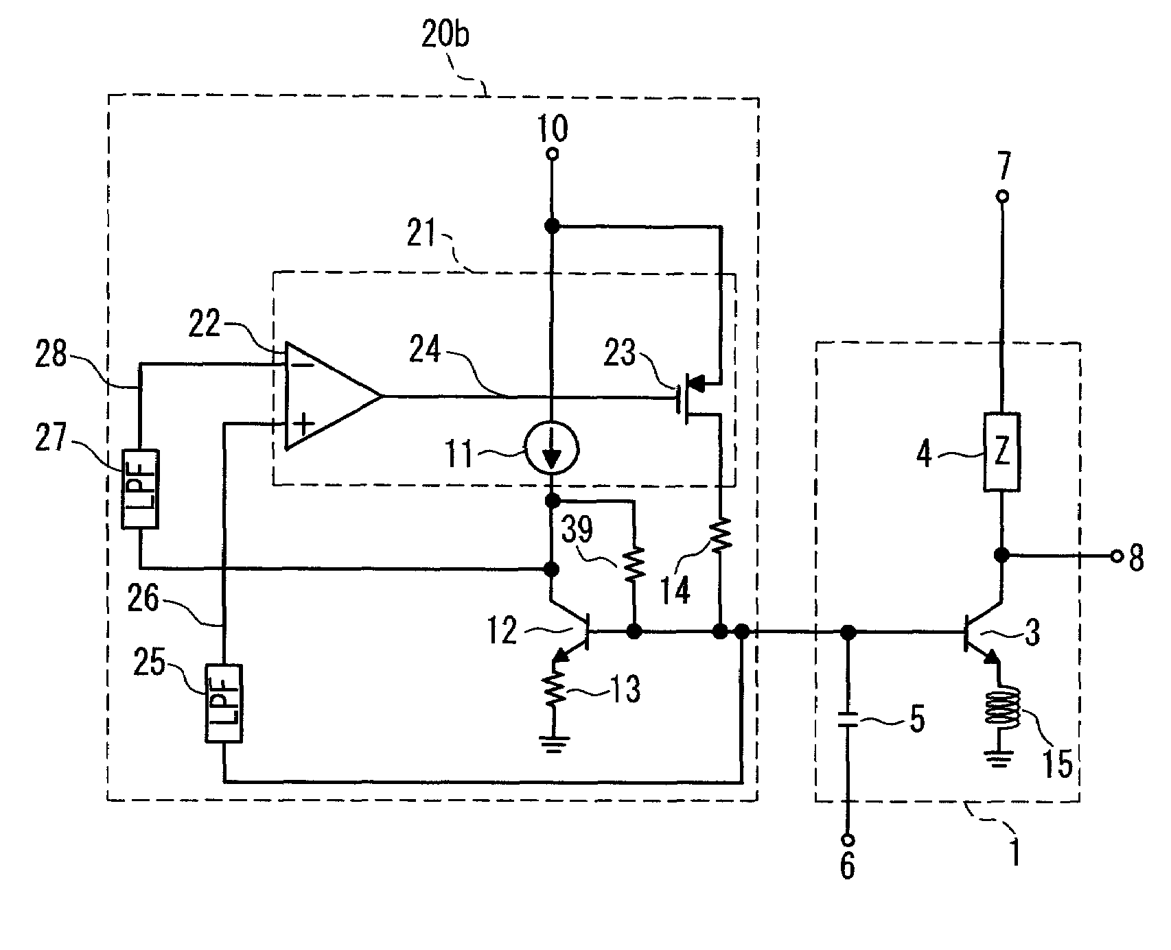
[0048]FIG. 6 is a circuit diagram showing a power amplifier according to a second embodiment of the present invention. In FIG. 6, the same reference numerals will be assigned to like elements in the circuit according to the first embodiment shown in FIG. 2, and redundant description will be omitted.

[0049]In this embodiment, a DC bias circuit 20b has a configuration in which a starting resistor 39 is inserted between the collector and the base of the current reference transistor 12 in the circuit according to the first embodiment. Hereinafter, an operation of this power amplifier will be described.

[0050]In a case where the starting resistor 39 is not provided, the base potential of the current reference transistor 12 is substantially 0 V when the power source is turned on. Therefore, it will take more time for equalizing the collector potential and the base potential of the current reference transistor 12 based on a feedback from the operational amplifier 22. On the contrary, the dif...

embodiment 3

[0053]FIG. 7 is a circuit diagram showing a power amplifier according to a third embodiment of the present invention. In FIG. 7, the same reference numerals will be assigned to like elements in the circuit according to the first embodiment shown in FIG. 2, and redundant description will be omitted.

[0054]In this embodiment, a DC bias circuit 20c has a configuration in which a phase adjusting section 40 is inserted between the first input 26 of the operational amplifier 22 and the base of the current reference transistor 12 in the circuit according to the first embodiment, and a phase adjusting section 41 is inserted between the second input 28 of the operational amplifier 22 and the collector of the current reference transistor 12. It is not necessarily required to provide the phase adjusting sections 40, 41 to both the first input 26 and the second input 28, and the phase adjusting section may be inserted into either one of the inputs. Hereinafter, an operation of this power amplifi...


PUM


Abstract

The present invention provides a power amplifier that includes the following: an RF operation transistor 3 having a base to which an RF signals is inputted, an emitter connected to the ground, and a collector connected to a power supply and a terminal for outputting an RF signal; a current reference transistor 12 having a collector connected to a reference current source 11, an emitter connected to the ground, and a base connected to the base of the RF operation transistor, an operational amplifier 22 formed of CMOS having one input connected to the collector of the current reference transistor and the other input connected to the base of the RF operation transistor; and a voltage-to-current conversion transistor 22 for converting the output of the operational amplifier 22 into a current to be supplied to the base of the RF operation transistor. The power amplifier has low power consumption and an efficient use of chip area, and a current variation due to the relative variation in hFE can be prevented, so as to be driven with a low power supply voltage.

Description

BACKGROUND OF THE INVENTION[0001]1. Field of the Invention[0002]The present invention relates to a power amplifier used mainly in various kinds of radio equipment, communication equipment, measuring devices, and the like.[0003]2. Description of Related Art[0004]FIG. 1 shows the circuit configuration of a conventional amplifier disclosed in, for example, JP 2004-153378. This amplifier includes an RF operation section 1 and a DC bias circuit 2.[0005]The RF operation section 1 includes an RF operation transistor 3 for carrying out voltage-to-current conversion, an impedance 4, a DC blocking capacitor 5, and a feedback inductor 15. The emitter of the RF operation transistor 3 is grounded via the feedback inductor 15, and the base of the RF operation transistor 3 is connected via the DC blocking capacitor 5 to an RF signal input terminal 6 to which a high frequency signal is inputted. A voltage is supplied from a power supply 7 to the collector of the RF operation transistor 3 via the im...

Claims


Application Information

Patent Timeline
Patent Type & Authority Patents(United States)
IPC IPC(8): H03F3/04
CPCH03F1/30H03F3/195H03F3/3022H03F3/45183H03F2200/513H03F2200/18H03F2200/451H03F2200/492
Inventor NAKAMURA, SHIGEKIITO, JUNJI
Owner PANASONIC SEMICON SOLUTIONS CO LTD
Why Eureka
Try Eureka