Scanning optical system

a scanning optical and optical system technology, applied in the field of scanning optical systems, can solve the problems of deterioration of image formation precision, fluctuation of scan lines formed on the image formation surface, loss of shape, etc., and achieve the effect of reducing the deterioration of diffraction efficiency

Inactive Publication Date: 2006-05-09
ASAHI KOGAKU KOGYO KK
View PDF18 Cites 0 Cited by
  • Summary
  • Abstract
  • Description
  • Claims
  • Application Information

AI Technical Summary

Benefits of technology

[0009]The present invention which has been made in consideration of the above problems is advantageous in that a scanning optical system employing a molded resin lens having a diffracting lens surface (on which the diffractive level difference structure is formed by injection molding of resin) can be provided while reducing the deterioration in the diffraction efficiency and the peripheral brightness caused by the deformation of the diffractive level difference structure due to the contraction of the resin in the injection molding process.
[0011]By the above configuration, an effective diameter of the diffracting lens surface (through which the beam scanning a range (effective scan width) on the image formation surface passes) measured in the main scanning direction can be kept substantially within a range 18 mm–28 mm. By keeping the effective diameter of the diffracting lens surface below the upper limit, displacement of each part of the resin due to the thermal contraction in the injection molding process can be kept low and the stress concentration occurring to each edge of the diffractive level difference structure can be kept to a minimum, by which the deformation (loss of shape) of the diffractive level difference structure can be prevented from occurring and the deterioration in the diffraction efficiency and the peripheral brightness caused by the deformation of the diffractive level difference structure can be reduced. On the other hand, by keeping the effective diameter of the diffracting lens surface above the lower limit, the possibility of deterioration in the optical performance and an increase in error sensitivity can be eliminated.
[0012]As above, by the present invention, a scanning optical system employing a molded resin lens having a diffracting lens surface (on which the diffractive level difference structure is formed by the injection molding of resin) can be provided, while reducing the deterioration in the diffraction efficiency and the peripheral brightness caused by the deformation (loss of shape) of the diffractive level difference structure due to the contraction of the resin in the injection molding process.

Problems solved by technology

Therefore, if the oscillation wavelength of the laser diode changes (due to individual differences, changes in the temperature and the output level, etc.), the length of each scan line formed on the image formation surface fluctuates due to chromatic aberration of magnification of the scan lens group, by which the precision of image formation is deteriorated.
However, even if the gate for injecting the resin into the mold is provided at the central position of the mold as described in the document #3, when a long lens having a lens surface with the diffractive level difference structure is manufactured by the injection molding of resin, deformation (e.g., loss of shape, getting out of shape) of the diffractive level difference structure tends to occur.
Due to such deformation of the edges, the diffractive level difference structure previously formed on the inner surface of the mold can not be transcribed correctly onto the lens surface, by which diffraction efficiency of the lens is deteriorated.

Method used


Image

  • Scanning optical system
  • Scanning optical system
  • Scanning optical system

Examples


first example

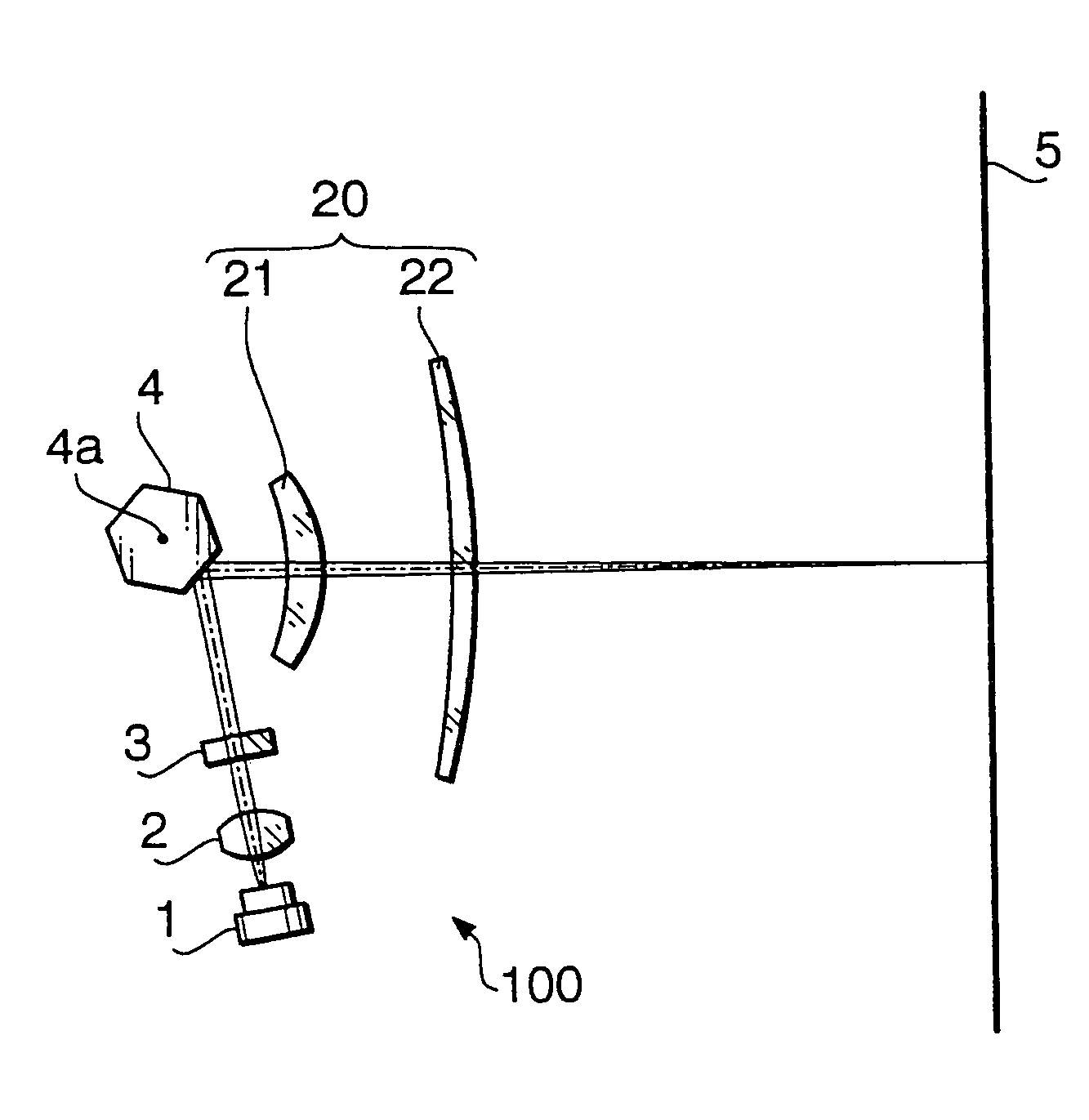
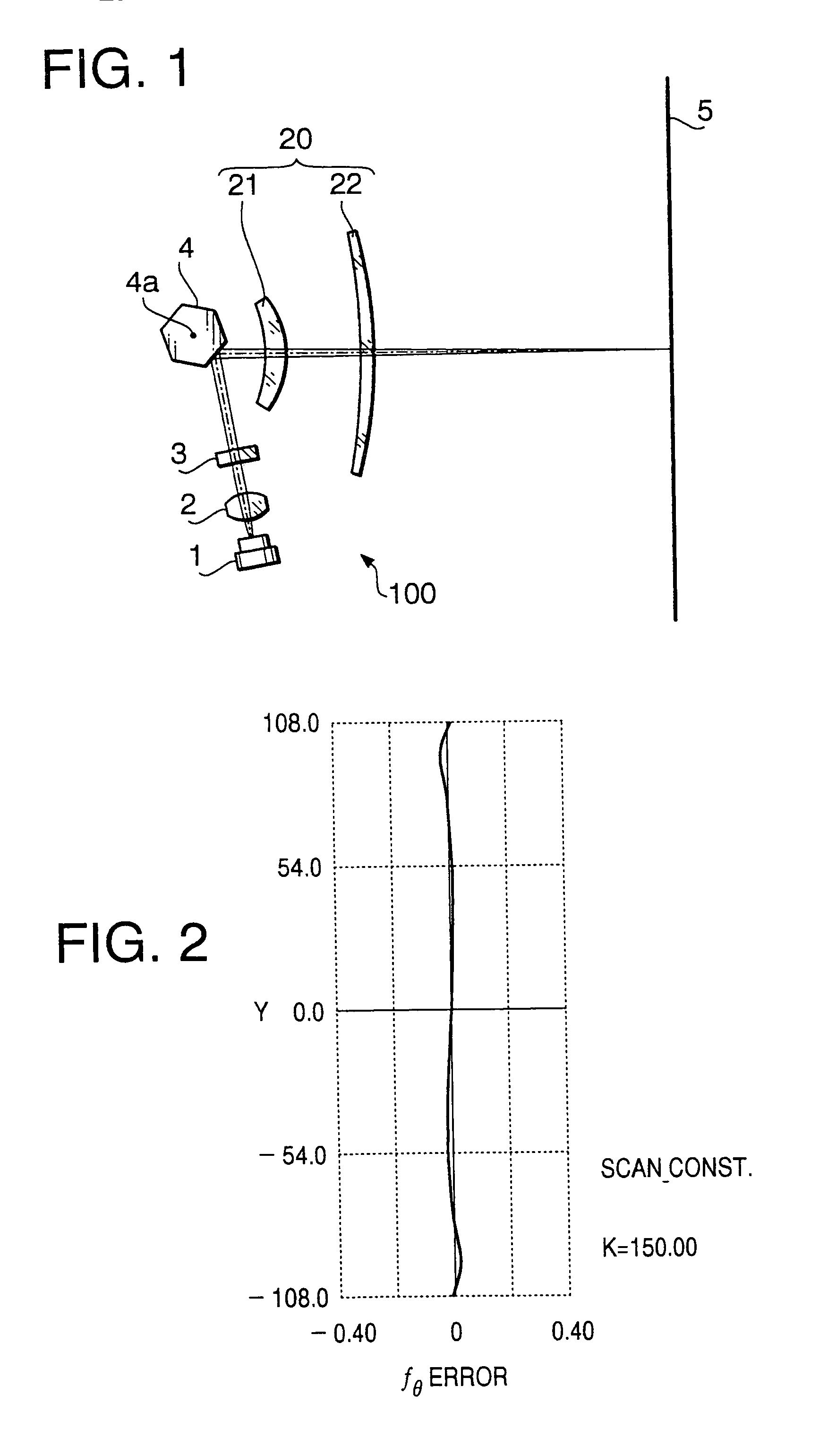
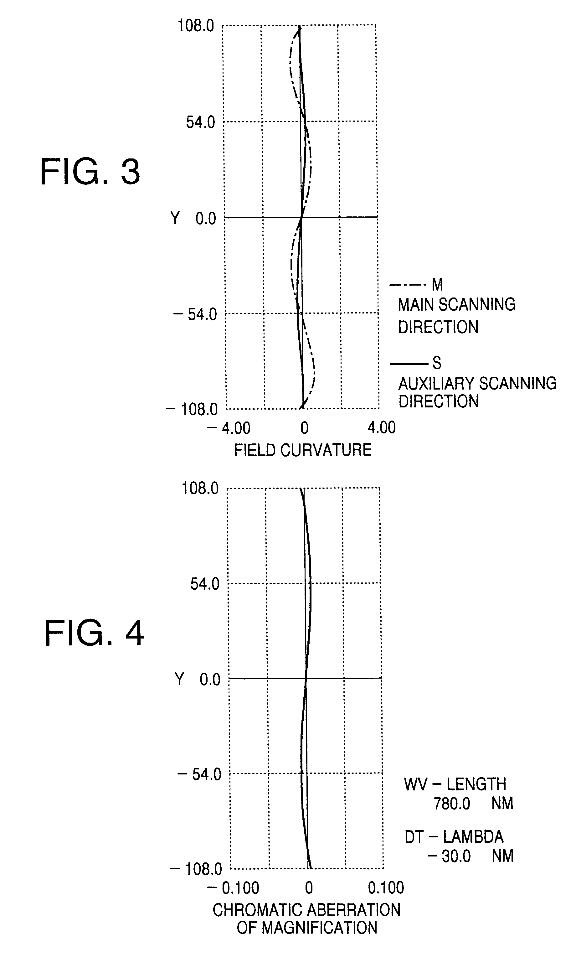
[0042]A scanning optical system as a first example of this embodiment is designed assuming that the wavelength of the laser beam emitted by the laser diode 1 is 780 nm. The focal length f of the fθ lens 20 regarding the main scanning direction is 150 mm, and the effective scan width W of the scanning optical system on the image formation surface is 216 mm. The polygon mirror 4 has six reflecting surfaces with an inscribed radius (the radius of the inscribed circle of the polygon) of 12.1 mm. The angle of the laser beam incident upon the polygon mirror 4 with respect to the optical axis of the fθ lens 20 is −80.0 degrees (“−”denotes the clockwise direction in FIG. 1).

[0043]The following Table 1 shows the configuration of each optical surface of the scanning optical system of the first example between the cylindrical lens 3 and the image formation surface 5. In the table, the symbol “R” denotes a curvature radius (mm) of each optical surface in the main scanning direction, “Rz” denote...

second example

[0058]Similarly to the first example described above, a scanning optical system as a second example of this embodiment is designed assuming the wavelength 780 nm of the laser beam emitted by the laser diode 1. The focal length f of the fθ lens 20 regarding the main scanning direction is 150 mm, and the effective scan width W of the scanning optical system on the image formation surface is 216 mm. The polygon mirror 4 has six reflecting surfaces with an inscribed radius of 12.1 mm. The angle of the laser beam incident upon the polygon mirror 4 with respect to the optical axis of the fθ lens 20 is −80.0 degrees (“−”denotes the clockwise direction in FIG. 1).

[0059]The following Table 4 shows the configuration of each optical surface of the scanning optical system of the second example between the cylindrical lens 3 and the image formation surface 5. The meaning of each symbol in Table 4 is the same as that in Table 1.

[0060]

TABLE 4No.RRzDn(780 nm)n(750 nm)#1∞33.204.001.51071.5107#2∞62.3...

third example

[0066]Similarly to the first and second examples described above, a scanning optical system as a third example of this embodiment is designed assuming the wavelength 780 nm of the laser beam emitted by the laser diode 1. The focal length f of the fθ lens 20 regarding the main scanning direction is 150 mm, and the effective scan width W of the scanning optical system on the image formation surface is 216 mm. The polygon mirror 4 has six reflecting surfaces with an inscribed radius of 12.1 mm. The angle of the laser beam incident upon the polygon mirror 4 with respect to the optical axis of the fθ lens 20 is −80.0 degrees (“−”denotes the clockwise direction in FIG. 1).

[0067]The following Table 7 shows the configuration of each optical surface of the scanning optical system of the third example between the cylindrical lens 3 and the image formation surface 5. The meaning of each symbol in Table 7 is the same as that in Table 1.

[0068]

TABLE 7No.RRzDn(780 nm)n(750 nm)#1∞33.204.001.51071.5...


PUM


Abstract

A scanning optical system comprises: a light source which emits a beam of light; a deflecting system that dynamically deflects the beam emitted by the light source with its deflecting surface; and a scan lens group including a molded resin lens, which focuses the beam dynamically deflected and scanned in a main scanning direction by the deflecting system on an image formation surface. In the scanning optical system, the molded resin lens has a diffracting lens surface which is provided with a diffractive level difference structure formed on a base curve having refractive power, and a following condition is satisfied:18<WL / P<28where “W” denotes an effective scan width (mm) on the image formation surface, “L” denotes a distance (mm) from the deflecting surface to the molded resin lens, and “P” denotes a distance (mm) from the deflecting surface to the image formation surface.

Description

INCORPORATION BY REFERENCE[0001]This application claims priority of Japanese Patent Application No. 2004-218407, filed on Jul. 27, 2004, the entire subject matter of the application being incorporated herein by reference.BACKGROUND OF THE INVENTION[0002]The present invention relates to a scanning optical system used for an image formation device such as a laser printer.[0003]In a scanning optical system, a beam of light emitted by a light source such as a laser diode is dynamically deflected (scanned) by a deflecting system such as a polygon mirror, and the beam scanned by the deflecting system is focused by a scan lens group such as an fθ lens to form a spot on an image formation surface of a photosensitive drum, etc. The spot which is scanned in a main scanning direction repetitively on the image formation surface successively forms a scan line on the image formation surface. Therefore, with the scanning optical system, by moving the image formation surface relative to the scannin...

Claims


Application Information

Patent Timeline
Patent Type & Authority Patents(United States)
IPC IPC(8): G02B26/08
CPCG02B26/125G02B3/08
Inventor TAKAKUBO, YUTAKA
Owner ASAHI KOGAKU KOGYO KK
Why Eureka
Try Eureka