Systems and methods for defect testing of externally accessible integrated circuit interconnects

a technology of external access and integrated circuit, which is applied in the field of integrated circuits, can solve the problems of limiting the testing of an integrated circuit b>100/b> to spot checks, difficult to test an integrated circuit at the die level, and impractical to move the test prob

Inactive Publication Date: 2009-11-03
MICRON TECH INC
View PDF12 Cites 10 Cited by
  • Summary
  • Abstract
  • Description
  • Claims
  • Application Information

AI Technical Summary

Problems solved by technology

It can be difficult to test an integrated circuit at the die level.
For example, physical test equipment limitations, such as the number of test equipment probes available to make contact with pads on the die, can limit the testing of an integrated circuit 100 to spot checks.
Time constraints for testing may render it impractical to move the test probe 102 to other pads.
Thus, defects can go undetected, and defective die can be delivered, packaged, combined with other chips, or the like.

Method used


Image

  • Systems and methods for defect testing of externally accessible integrated circuit interconnects
  • Systems and methods for defect testing of externally accessible integrated circuit interconnects
  • Systems and methods for defect testing of externally accessible integrated circuit interconnects

Examples


Embodiment Construction

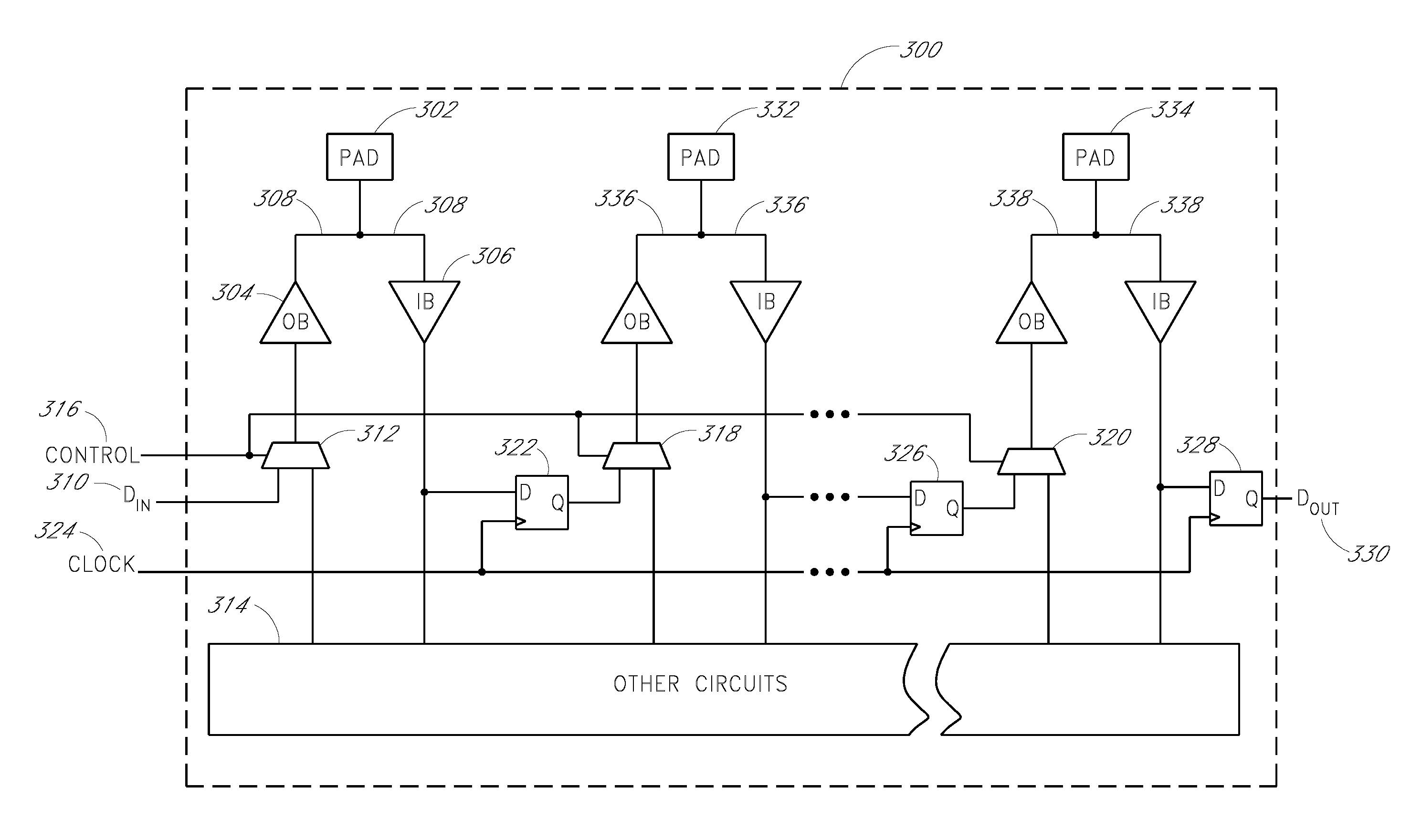
[0015]Apparatus and methods provide built-in testing enhancements in integrated circuits. This permits more thorough testing of integrated circuits at the die level. For example, techniques to test continuity between externally accessible interconnects and internal circuitry are disclosed. Also disclosed are techniques to test leakage current of multiple externally accessible interconnects, including one or more externally accessible interconnects not directly probed. While illustrated in the context of pads for the externally accessible interconnects, the skilled artisan will appreciate that the principles and advantages described herein are applicable to other types of externally acessible interconnects. Although particular embodiments are described herein, other embodiments of the invention, including embodiments that do not provide all of the benefits and features set forth herein, will be apparent to those of ordinary skill in the art.

[0016]In one embodiment, a test signal is r...


PUM


Abstract

Apparatus and methods provide built-in testing enhancements in integrated circuits. These testing enhancements permit, for example, continuity testing to pads and / or leakage current testing for more than one pad. The disclosed techniques may permit more thorough testing of integrated circuits at the die level, thereby reducing the number of defective devices that are further processed, saving both time and money. In one embodiment, a test signal is routed in real time through a built-in path that includes an input buffer for a pad under test. This permits testing of continuity between the pad and the input buffer. An output buffer can also be tested as applicable. In another embodiment, two or more pads of a die are electronically coupled together such that leakage current testing applied by a probe connected to one pad can be used to test another pad.

Description

BACKGROUND[0001]1. Field of the Invention[0002]Embodiments of the invention generally relate to integrated circuits. In particular, embodiments of the invention relate to circuits that facilitate the identification of defective circuits.[0003]2. Description of the Related Art[0004]Integrated circuit (IC) devices are typically tested for defects at various stages of production. Typically, the tests become more complete as the chip progresses through production. While virtually all IC devices are eventually tested thoroughly, it is desirable to catch defects as early as possible, for example, before the die is assembled in a package. Dies for an integrated circuit can also be delivered prior to packaging. For example, multiple memory chips are frequently packaged together in a single package. In addition, multiple dies are frequently combined and assembled in a single package known as a hybrid.[0005]It can be difficult to test an integrated circuit at the die level. For example, physi...

Claims


Application Information

Patent Timeline
Patent Type & Authority Patents(United States)
IPC IPC(8): G01R31/28G01R31/04
CPCG01R31/31715G01R31/31717G11C29/022G11C29/1201G11C29/56G11C29/02G01R31/3004G11C2029/5006
Inventor FUJIWARA, YOSHINORINOMURA, MASAYOSHI
Owner MICRON TECH INC
Why Eureka
Try Eureka