Memory device and method of operating such a memory device

a memory device and memory technology, applied in the field of memory devices and methods of operating such memory devices, can solve the problems of significant failure rate, adversely affecting the predictability of operation, and increasing the behavior of individual memory cells, so as to increase the read current through the memory cell, and increase the stability of the addressed memory cell

Active Publication Date: 2009-11-03
ARM LTD
View PDF3 Cites 23 Cited by
  • Summary
  • Abstract
  • Description
  • Claims
  • Application Information

AI Technical Summary

Benefits of technology

[0017]In accordance with the present invention, advantage is taken of the existing cross capacity which is already present in a standard memory cell. In particular, for each column, a capacitance exists between the supply voltage line for that column and the associated bit line or pair of bit lines for that column. In accordance with the present invention, this is utilised to bring about a change in the voltage level on the supply voltage line during certain memory access operations. In particular, for a predetermined period during the memory access operation, control circuitry is used to disconnect from the voltage source the supply voltage line for at least a selected column. Accordingly, when the voltage level changes on an associated bit line, the cross capacitance between the bit line and the supply voltage line brings about a change in voltage level on the supply voltage line that can be used to assist correct operation in a variety of memory access operations.
[0041]In embodiments where a pair of bit lines are associated with each column, in one embodiment one of the bit lines can be discharged prior to the precharge operation associated with the read operation such that when that bit line is subsequently precharged, this gives a boost to the supply voltage level on the supply voltage line. However, if desired, both of the bit lines in the pair can be discharged, so that during the precharge operation both of them are precharged back up to VDD, this giving a further increase to the voltage on the supply voltage line, thereby further improving stability and increasing read current in the subsequent read stage of the operation.

Problems solved by technology

However, as the memory cells decrease in size, the variation in behaviour between individual memory cells tends to increase, and this can adversely affect predictability of operation.
This variation in operation of the individual memory cells can give rise to significant failure rates when trying to run the memory devices at high speed to meet the performance requirements.
It is often also the case that there is a desire to use a lower power supply voltage for the memory device in order to reduce power consumption, but this can further increase the likelihood of failed operation within individual memory cells.
Accordingly, in modern technologies, it is becoming more and more difficult to produce memory devices where the individual memory cells have the required stability to ensure effective retention of data (stability sometimes being measured in terms of static noise margin (SNM)), whilst also having required write-ability (WM) to ensure that new data values can be stored in the cells within the time period allowed for a write operation.
However, the implementation disclosed in FIG. 1 has a number of problems.
Firstly, the time available to lower the supply voltage during the write operation is extremely limited, due to the short time available for performing write operations in high performance memory devices.
The charge that needs to be dissipated when reducing the voltage on the supply line hence leads to large current peaks.
Further, the memory requires for every output bit the use of a column with the supply voltage lowered, and this accordingly increases the current peak problem mentioned above.
Such voltage generators will also be susceptible to temperature and voltage variations, which may require correcting circuits to be added.
In addition to these problems, in memory devices designed for low power applications, the presence of the additional voltage generator leads to significant power consumption since the additional voltage supply must be maintained at all times to enable that supply voltage to be available ahead of any write operation.
A disadvantage of such an approach is that a significant DC current is produced by the band gap generator circuitry used, and power is lost in charging and discharging the column supply line with different voltages every write cycle.
Hence, such an approach is likely to be unacceptable in many memory devices, for example those designed for low power applications.
Further, the band gap generator and push-pull transistor stage consume valuable space within the memory device.
Whilst this approach can reduce the voltage on the column supply voltage line very quickly, it does require the provision of an extra metal line within the memory circuit, along with the use of a pre-charge circuit in association with that extra line to precharge that line to a ground level, giving rise to power loss associated with such precharge circuits.
The provision of such an additional line is likely to increase cost, and may prove difficult to incorporate within high density memory designs.
Further, the increase in power consumption associated with the precharge circuits provided for that additional line may be unacceptable in certain memory devices, for example those designed for low power applications.
The disadvantages of such an approach are that it involves a significant modification to the standard SRAM memory cell, results in a non-regular layout which may prove difficult to implement, and will result in a slow read operation due to the use of a single bit line.

Method used


Image

  • Memory device and method of operating such a memory device
  • Memory device and method of operating such a memory device
  • Memory device and method of operating such a memory device

Examples


Embodiment Construction

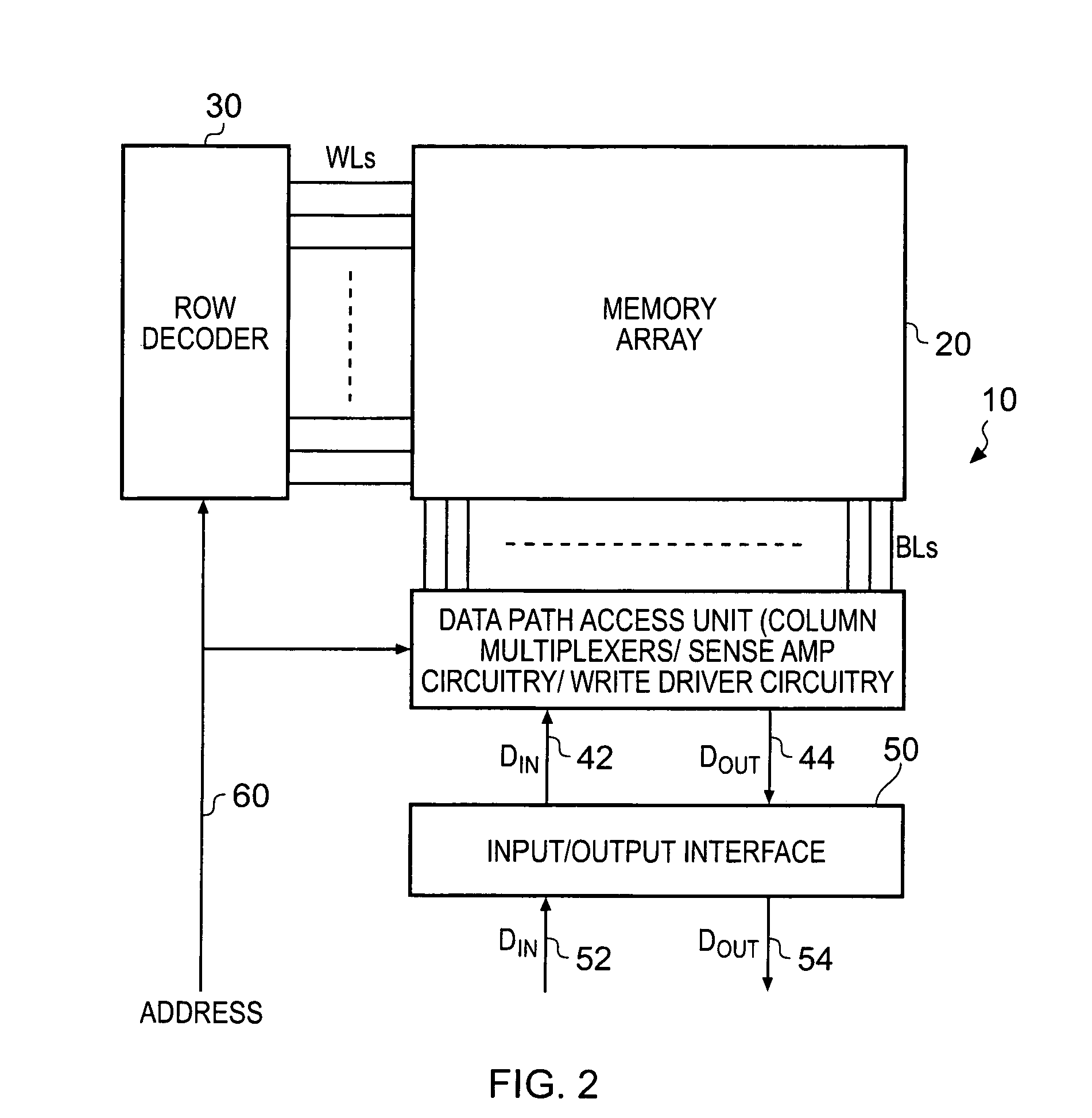
[0061]FIG. 2 is a block diagram of a memory device. The memory device 10 has a memory array 20 consisting of a plurality of memory cells arranged in rows and columns. Each row has a word line (WL) connected thereto, and each column has at least one bit line (BL) connected thereto, the exact number of bit lines connected to each column being dependent on the implementation. In one example implementation, the memory array consists of SRAM cells, and a pair of bit lines are connected to each column of cells.

[0062]When a memory access request is received by the memory device, the address specified by the memory access request is routed over path 60 to a row decoder 30 and to a data path access unit 40. The row decoder 30 is arranged to decode the address and dependent thereon drive a control signal over one of the word lines in order to select one of the rows within the memory array 20. Similarly, the data path access unit 40 is arranged dependent on the address to identify the column o...


PUM


Abstract

A memory device and method of operation is provided, the memory device having a plurality of memory cells arranged in at least one column, with each column having at least one bit line and a supply voltage line associated therewith. A capacitance exists between the supply voltage line and associated at least one bit line for each column. Control circuitry is used to control, for each column, connection of a voltage source to the associated supply voltage line. For a predetermined period during a memory access operation, the control circuitry disconnects the supply voltage line for at least the selected column from the voltage source, such that a voltage level on that supply voltage line changes in response to any change in voltage on the associated at least one bit line. This basic mechanism can be used to provide a variety of assist mechanisms, such as a write assist mechanism, a bit flip assist mechanism and a read assist mechanism. The technique of the present invention provides a particularly simple and power efficient technique for providing such assist mechanisms.

Description

BACKGROUND OF THE INVENTION[0001]1. Field of the Invention[0002]The present invention relates to a memory device and method of operating such a memory device, and in particular to techniques that can be employed when performing memory access operations to assist those memory access operations.[0003]2. Description of the Prior Art[0004]There is an increasing demand for memory devices to be constructed which are smaller and consume less power than their predecessor designs, whilst retaining high performance. New technologies are being developed which allow a reduction in size of the individual transistors making up each memory cell. However, as the memory cells decrease in size, the variation in behaviour between individual memory cells tends to increase, and this can adversely affect predictability of operation. This variation in operation of the individual memory cells can give rise to significant failure rates when trying to run the memory devices at high speed to meet the performa...

Claims


Application Information

Patent Timeline
Patent Type & Authority Patents(United States)
IPC IPC(8): G11C5/14
CPCG11C11/417
Inventor VAN WINKELHOFF, NICOLAAS KLARINUS JOHANNESDUFOURT, DENIS RENE ANDRE
Owner ARM LTD
Why Eureka
Try Eureka