Method of manufacturing non-volatile memory device
a non-volatile memory and manufacturing method technology, applied in the direction of semiconductor devices, basic electric elements, electrical appliances, etc., can solve the problems of increased leakage current of high-voltage transistors in the peripheral region, hump characteristic generation, and high-voltage transistor malfunctions, etc., to reduce the step
- Summary
- Abstract
- Description
- Claims
- Application Information
AI Technical Summary
Benefits of technology
Problems solved by technology
Method used
Image
Examples
Embodiment Construction
[0010]A specific embodiment according to the present patent will be described with reference to the accompanying drawings.
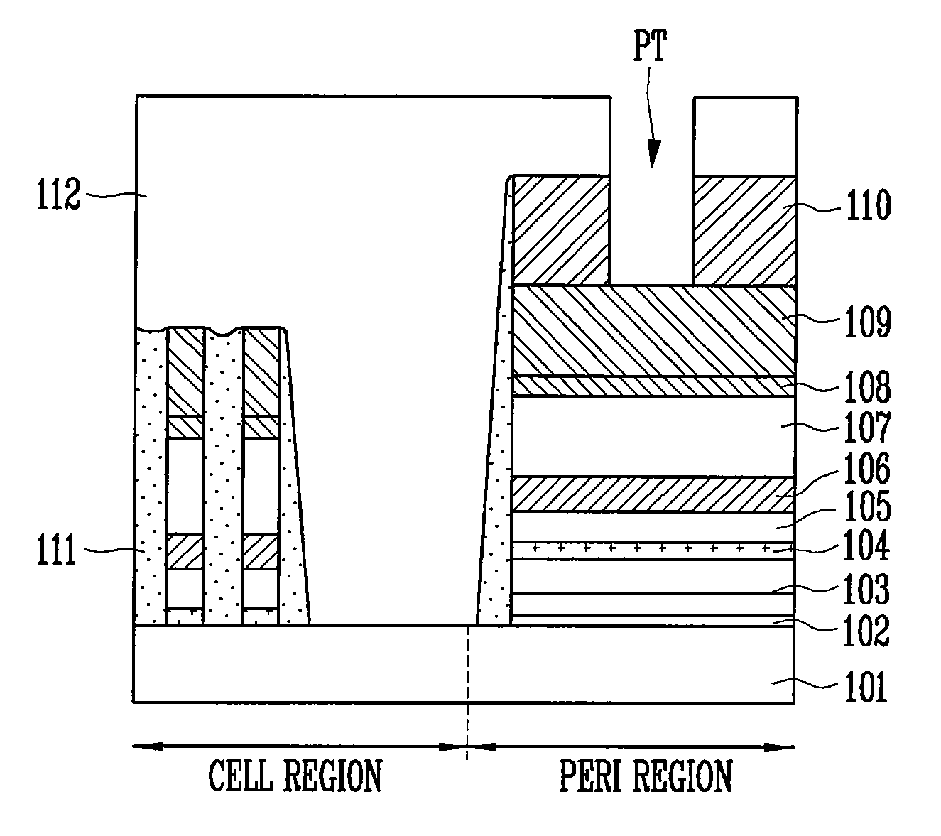
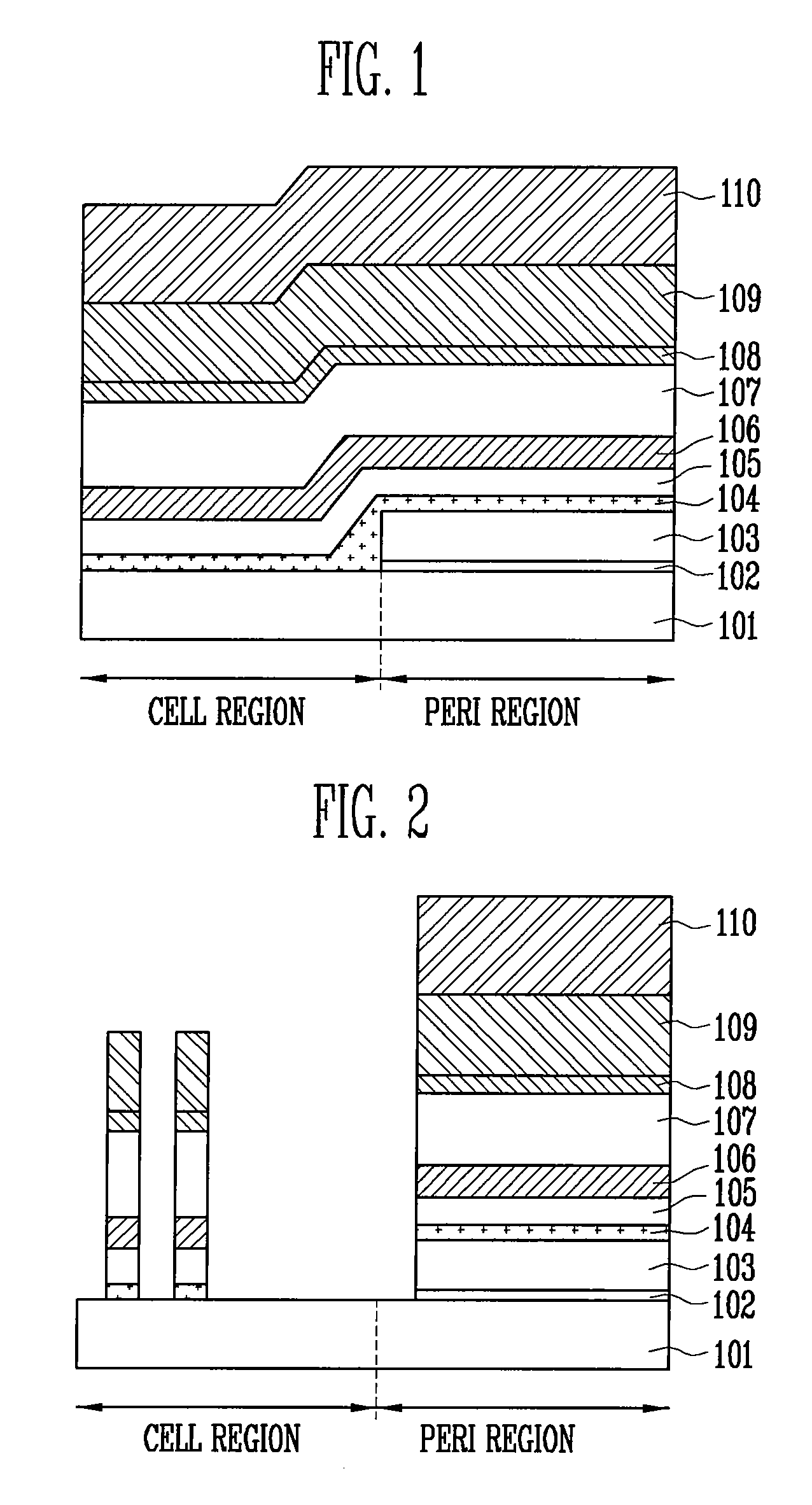
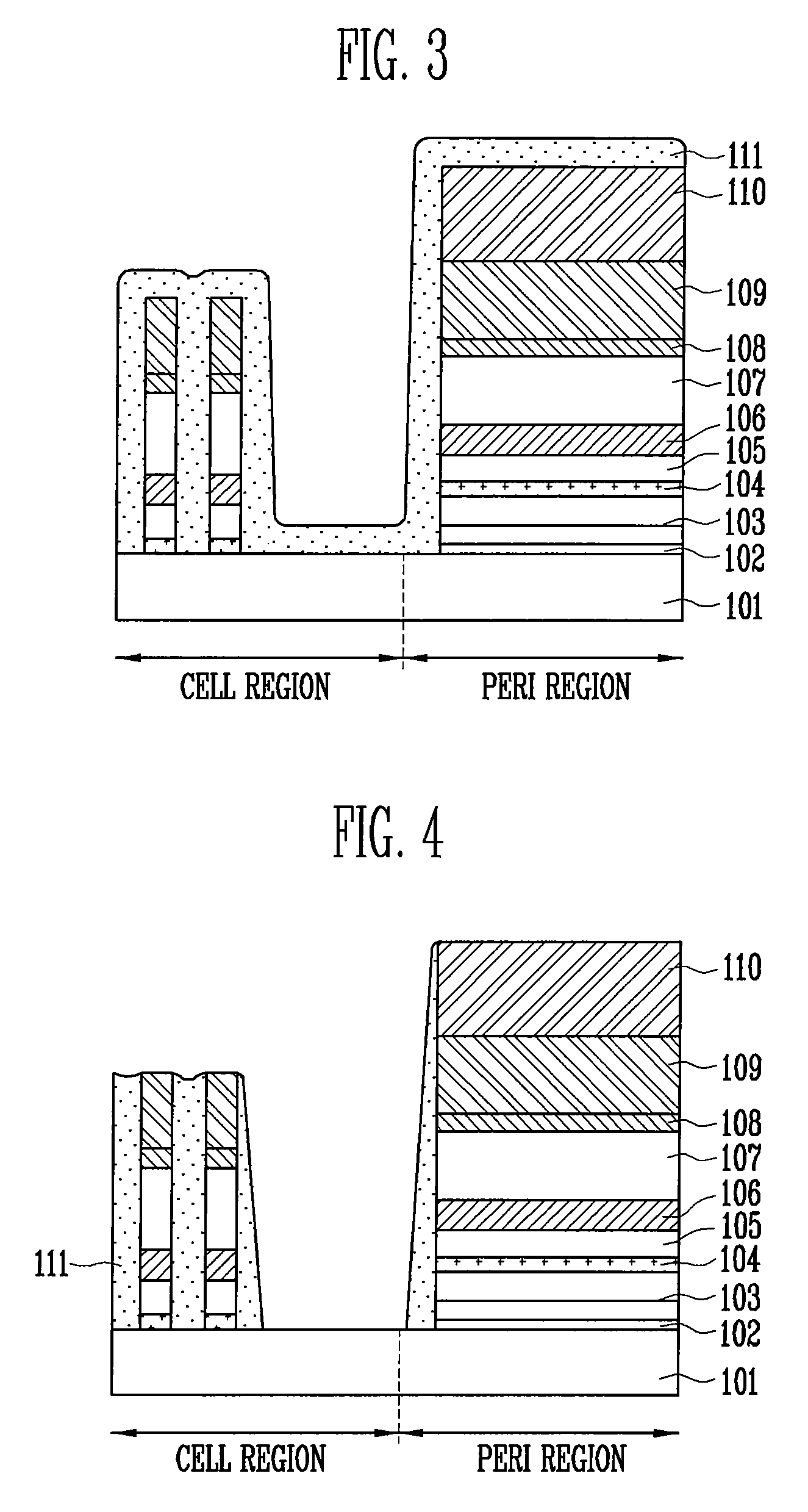
[0011]Referring to FIG. 1, a gate insulating layer 102 and a first conductive layer 103 are formed in a peripheral region of a semiconductor substrate 101. A dielectric layer 104, a capping polysilicon layer 105, a second conductive layer 106, a tungsten silicide layer 107, a SiON layer 108, a hard mask 109 and a carbon hard mask 110 are sequentially laminated over the semiconductor substrate including the first conductive layer 103. The first conductive layer 103 and the second conductive layer 106 are formed from polysilicon. The gate insulating layer 102 and the first conductive layer 103 can be formed to a thickness of about 70 and 800 angstroms, respectively. Furthermore, the dielectric layer 104 can have an ONO (oxide-nitride-oxide) structure. The ONO structure comprises a lamination structure of a lower oxide layer, a nitride layer and an upper oxide layer...
PUM
 Abstract
Description
Claims
Application Information


