Optical waveguide bio-sensing device

a biosensing device and optical waveguide technology, applied in the field of optical waveguide biosensing devices, can solve the problems of inability to provide dynamic information of real-time interaction, inability to detect high-sensitivity interactions, etc., to achieve the effect of simplifying the optical system using the present invention and high sensitivity detection techniques

Inactive Publication Date: 2009-12-22
IND TECH RES INST
View PDF6 Cites 6 Cited by
  • Summary
  • Abstract
  • Description
  • Claims
  • Application Information

AI Technical Summary

Benefits of technology

[0009]It is a primary object of the present invention to provide an optical waveguide bio-sensing device, using a grating chip with a sub-wavelength grating to serve as a platform for molecular interaction so as to detect bio-molecular interactions, reaction rate and / or molecular dynamics without any labeling in real time. Optical systems using the present invention are simplified and capable of being portable. Thus a high sensitivity detection technique is achieved.

Problems solved by technology

In fluorescence detection, problems related to complicated fluorescence tags, difficulty in molecule tags, inevitable fluorescence decay and unavailability in dynamics information of real-time interaction occur.
However, the reflectance spectrum exhibits a wide FWHM (full width at half magnitude) leading to a poor wavelength resolution so that detection in physiology concentration is unavailable.

Method used


Image

  • Optical waveguide bio-sensing device
  • Optical waveguide bio-sensing device
  • Optical waveguide bio-sensing device

Examples


first embodiment

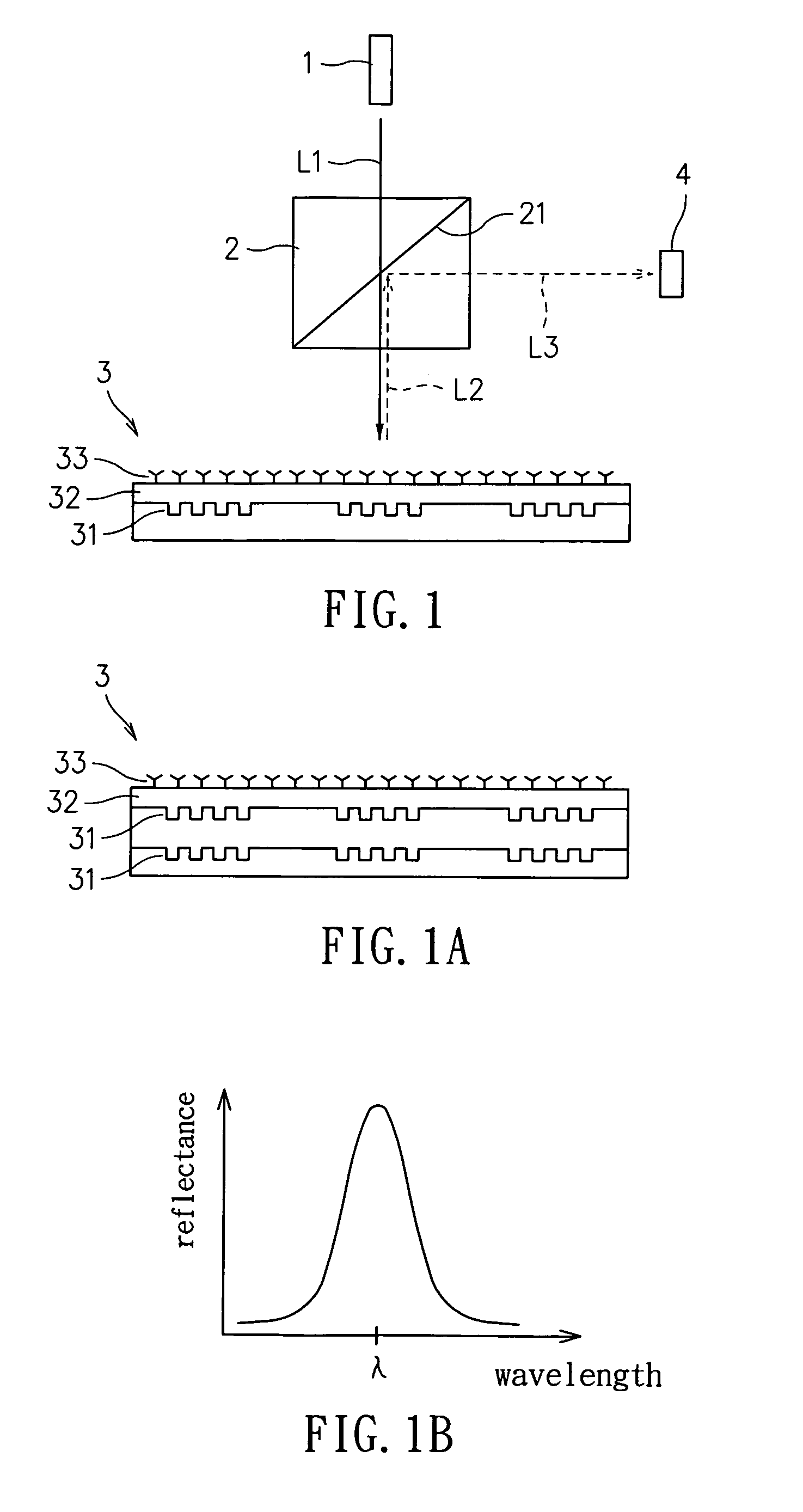
[0046]Please refer to FIG. 1, which is a schematic diagram showing an optical waveguide bio-sensing device wherein the grating chip not bounded with any bio-molecule according to the present invention. The optical waveguide bio-sensing device comprises a light source 1, a beam splitter 2, a grating chip 3 and a sensor 4. In the present invention, the light source 1 is a monochromatic laser or semiconductor light source with a wavelength λ within a range from 200 nm to 1700 nm. The beam splitter 2 with polarization is disposed on the optical path so that the monochromatic light with a wavelength λ travels through the beam splitter 2 and reaches the grating chip 3. The grating structure 3 comprising at least a grating structure 31 and a waveguide layer 32 on the grating structure 31 for receiving the monochromatic light split by the beam splitter 2, wherein a receptor 33 is provided on the waveguide layer 32. The grating structure 31 is a low refractive index grating structure. The gr...

second embodiment

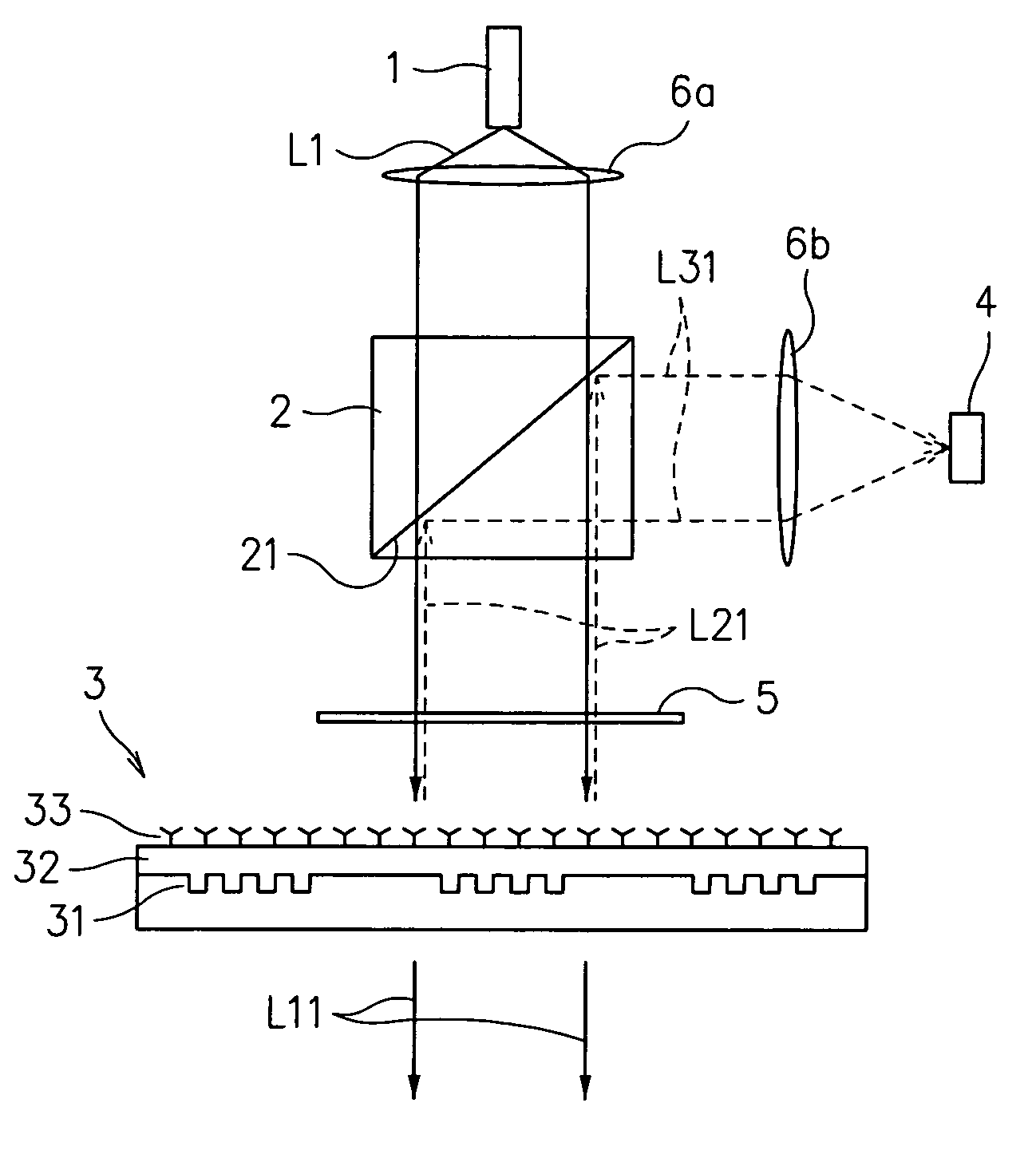
[0049]Please refer to FIG. 3, which is a schematic diagram showing an optical waveguide bio-sensing device wherein the grating chip is not bounded with any bio-molecule according to the present invention. The optical waveguide bio-sensing device comprises a light source 1, a beam splitter 2, a grating chip 3 and a sensor 4. In the present embodiment, a first light concentrating element 6a is disposed between the light source 1 and the beam splitter 2 for light concentration and a second light concentrating element 6b is disposed between the grating chip 3 and the sensor 4 for light concentration. The light concentrating elements 6a and 6b can be implemented using lenses with light concentration. Moreover, in order to enhance the sensitivity of the system using the optical waveguide bio-sensing device, a quarter waveplate (¼λ) 5 is arranged in the optical path between the beam splitter 2 and the grating chip 3.

[0050]Therefore, the monochromatic light L1 emitted from the light source ...

third embodiment

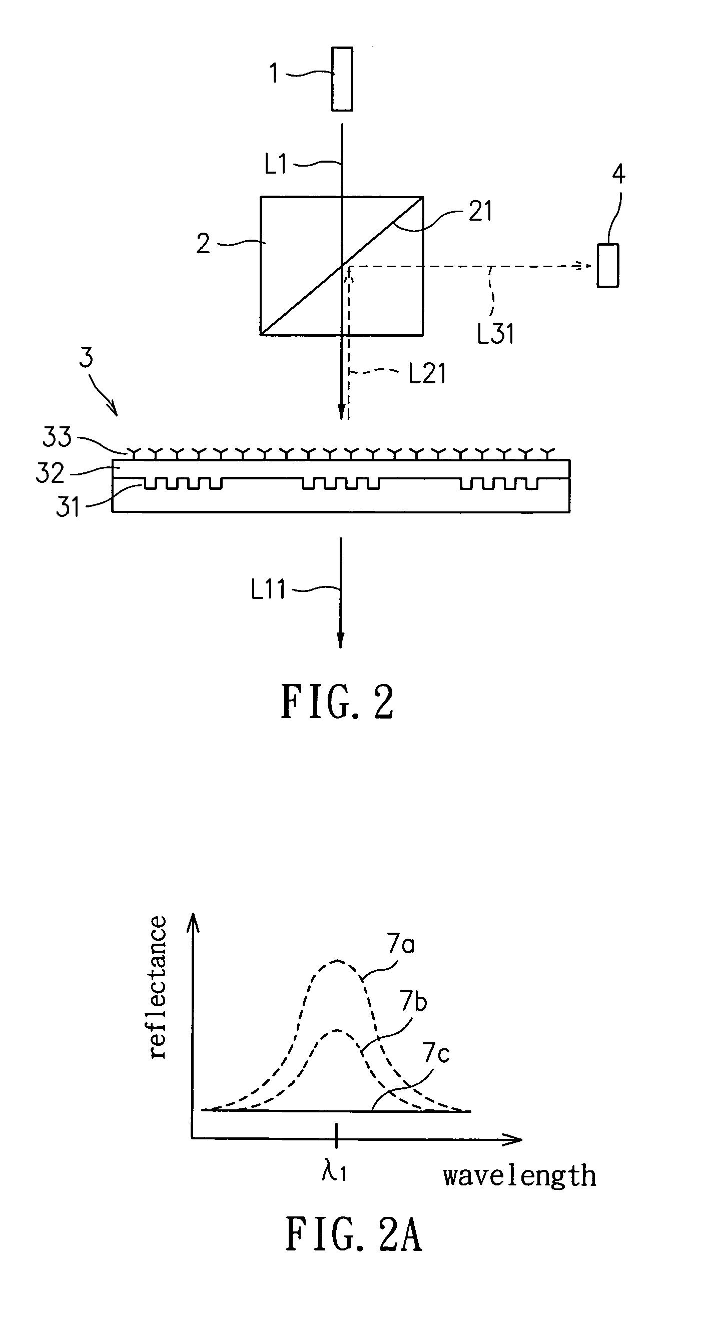
[0052]Please refer to FIG. 5, which is a schematic diagram showing an optical waveguide bio-sensing device wherein the grating chip is not bounded with any bio-molecule according to the present invention. The optical waveguide bio-sensing device comprises a light source 1, a beam splitter 2, a grating chip 3, a sensor 4, a quarter waveplate 5 and light concentrating elements 60a and 60b. In the present embodiment, and quarter waveplate 5 and light concentrating elements 60a and 60b are disposed on the surfaces of the beam splitter 2. The quarter waveplate 5 is a planar surface with polarization and the light concentrating elements 60a and 60b are Fresnel surfaces with light concentration. Referring to FIG. 5A for a cross-sectional view of a Fresnel surface, the Fresnel surface comprises a plurality of concentric circular ridges. These circular ridges give the Fresnel surface a zigzag or sawtooth cross-section. Each sawtooth creates a tiny prism. By choosing appropriate powers for th...


PUM


Abstract

An optical waveguide bio-sensing device, comprising: a monochromatic light source, a beam splitter, a grating chip with a sub-wavelength grating structure and a sensor. Moreover, in order to enhance the sensitivity of the system using the optical waveguide bio-sensing device, a light concentrating element or a quarter waveplate (¼λ) is arranged in the optical path during detection. When the grating chip is not coated with a layer of biochemical substance corresponding to a monochrome light emitted from the monochromatic light source, a reflected light of a specific narrow wavelength is reflected by a specific angle as a surface plasmon resonant effect caused by waveguide coupling is excited by the incidence of the monochrome light to the grating chip through the beam splitter; otherwise, there will be little or no reflection. Accordingly, the optical waveguide bio-sensing device can detect bio-molecular interactions, reaction rate and / or molecular dynamics without any labeling in real time. Optical systems using the present invention are simplified and capable of being portable. Thus a high sensitivity detection technique is achieved.

Description

BACKGROUND OF THE INVENTION[0001]1. Field of the Invention[0002]The present invention generally relates to an optical waveguide bio-sensing device and, more particularly, to an optical waveguide bio-sensing device using a grating chip with a sub-wavelength grating to serve as a platform for molecular interaction so as to detect bio-molecular interactions, reaction rate and / or molecular dynamics without any labeling in real time. Optical systems using the present invention are simplified and capable of being portable. Thus a high sensitivity detection technique is achieved.[0003]2. Description of the Prior Art[0004]Bio-technology is regarded as the most important field of research and the most potential industry that most countries have put emphasis upon. Bio-technology includes agricultural bio-technology, bio-pharmaceutical technology and genomic and therefore it is crucial in pharmaceutics, genomics and proteomics.[0005]In bio-molecular interaction analysis (BIA), bio-chips have a...

Claims


Application Information

Patent Timeline
Patent Type & Authority Patents(United States)
IPC IPC(8): G02B6/00G02B6/34
CPCG01N21/553G01N21/7703G01N2021/7773
Inventor MAO, YEN-CHIEHLIN, JIAN-SHIANCHEN, LAI-SHENGWANG, WEI-HAN
Owner IND TECH RES INST
Why Eureka
Try Eureka