Photoconductive element for radiation detection in a radiography imaging system

a radiation detection and radiography imaging technology, applied in the field of radiography imaging systems, can solve the problems of high dark current at higher electric fields, reduce fabrication yield, and drive up manufacturing costs, and achieve the effects of reducing the dark current of photoconductor, increasing the collection efficiency of electron hole pairs, and speeding up speed

Active Publication Date: 2015-09-17
DOSE SMART IMAGING
View PDF6 Cites 16 Cited by
  • Summary
  • Abstract
  • Description
  • Claims
  • Application Information

AI Technical Summary

Benefits of technology

[0008]The insulator layer placed between the semiconducting layer and lateral sensor contacts performs the function of reducing the dark current of photoconductor even when a high electric field is applied across the sensor contacts. Applying the high electric field enables the MISIM photoconductive element to operate at a faster speed than conventional metal-semiconductor-metal (MSM) photoconductor designs and also to increase the collection efficiency of the electron hole pairs created by the photons impinging on the semiconducting layer. The structure of the present invention is simpler and correspondingly less expensive to manufacture in comparison to a traditional photodiode structure. Moreover, unlike traditional MSM photoconductors, the structure of the present invention yields higher performance and can be realized in a large area display electronics manufacturing process. These and other advantages of the aspects of the present invention will be understood in conjunction with the following detailed description and accompanying drawings.

Problems solved by technology

The key challenges with fabricating a vertical photodiode are the modifications required to the thin film transistor fabrication process specifically, thick amorphous silicon layers, specialized p doped contact layer and a complex RIE sidewall etching process to prevent optical crosstalk.
These challenges reduce the fabrication yield and drive up the cost of manufacture.
The key challenges with fabricating a lateral MSM photoconductor include the high dark currents at higher electric fields and photoresponse non-uniformity due to a non-uniform electric field.
Both issues degrade performance, which is the key reason why MSM devices are not used in industry today for large area digital X-ray imaging.

Method used


Image

  • Photoconductive element for radiation detection in a radiography imaging system
  • Photoconductive element for radiation detection in a radiography imaging system
  • Photoconductive element for radiation detection in a radiography imaging system

Examples


Embodiment Construction

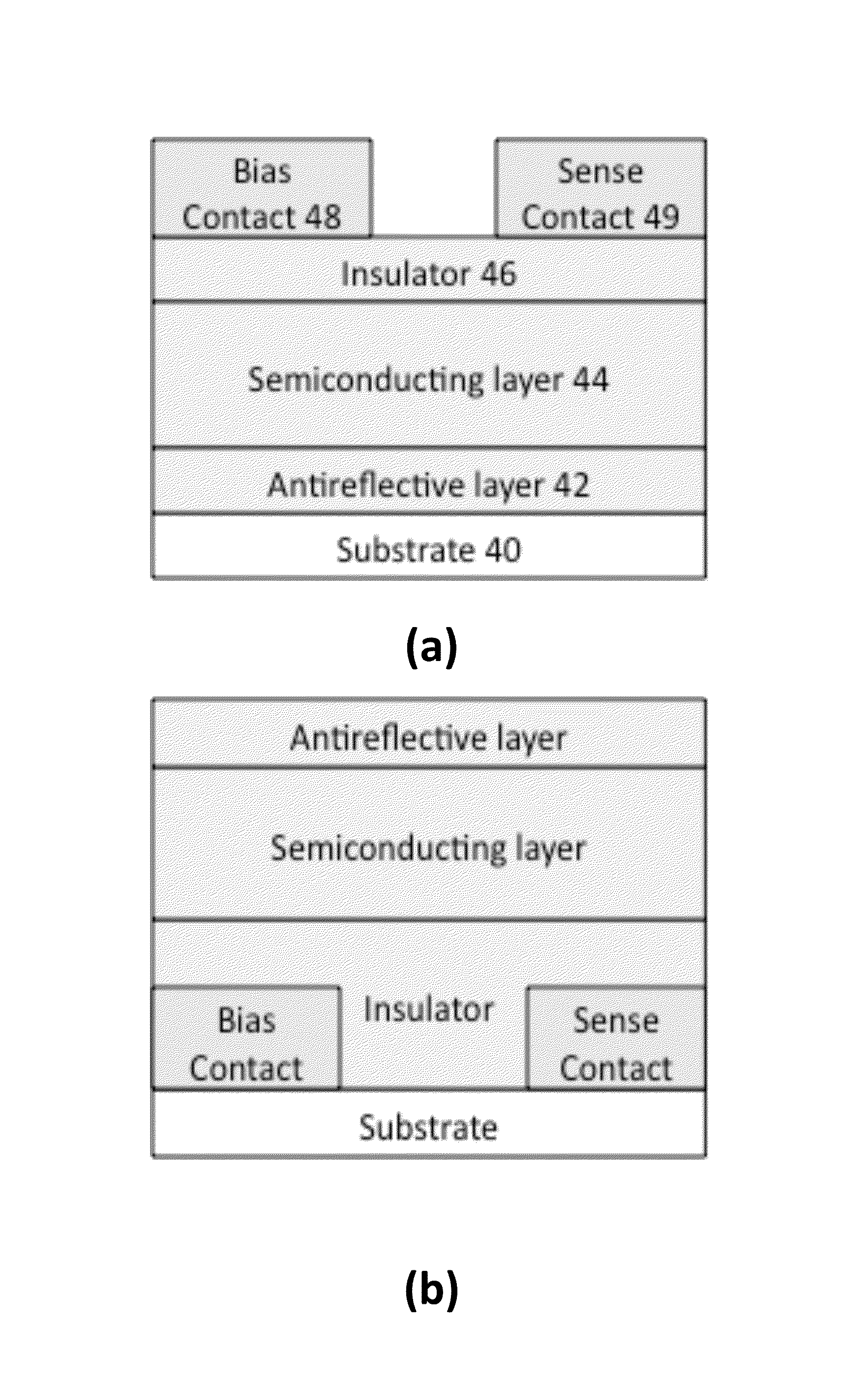
[0016]The present invention relates to a novel photoconductive element that includes a MISIM detector integrated with a switching element for a radiography imaging system. The following description is presented to enable one of ordinary skill in the art to make and use the invention and is provided in the context of a patent application and its requirements. Various modifications to the preferred embodiment will be readily apparent to those skilled in the art and the generic principles herein may be applied to other embodiments. Thus, the present invention is not intended to be merely limited to the embodiment shown but is to be accorded the widest scope consistent with the principles and features described herein.

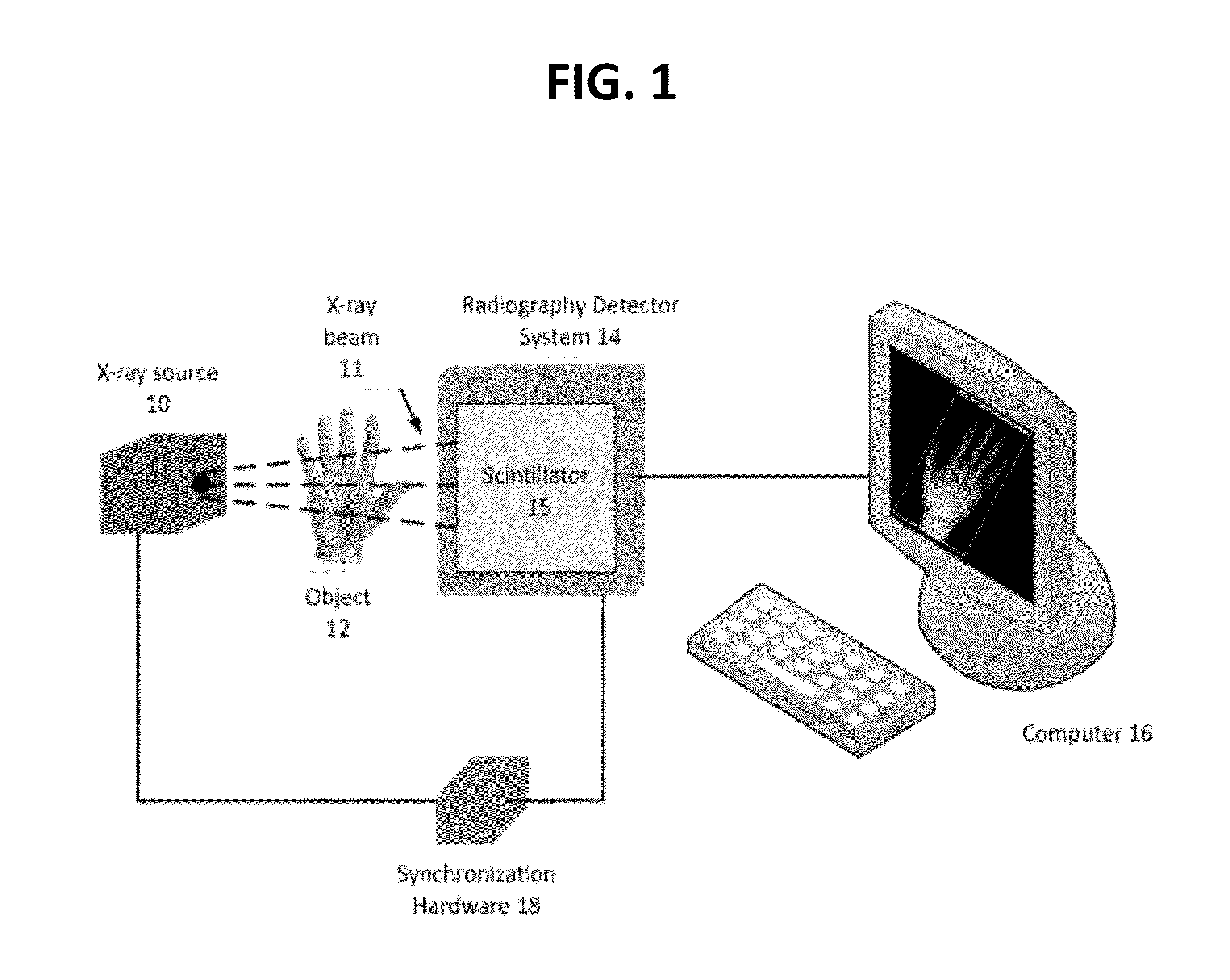
[0017]FIG. 1 illustrates a general diagram of a radiographic imaging environment in accordance with the present invention. As shown, an X-ray source 10 generates an X-ray beam 11 that is transmitted toward an object 12, e.g., a patient's hand, for imaging by a radiography ...


PUM


Abstract

This disclosure is directed at a photoconductive element for a digital X-ray imaging system which consists of a detector element comprising a semiconducting layer for absorbing photons, an insulator layer on at least one surface of said semiconducting layer and at least two electrodes on one surface of said insulator layer; and a switching element wherein at least one layer within said switching element is in the same plane as at least one said layer within said detector element.

Description

FIELD OF THE DISCLOSURE[0001]This invention relates to radiography imaging systems, and more particularly to a photoconductive detector using an insulating contact layer in a radiography imaging system.BACKGROUND OF THE DISCLOSURE[0002]Traditionally, X-ray diagnostic processes record x-ray image patterns on silver halide films. These systems direct an initially uniform pattern of impinging X-ray radiation through the object to be studied, intercept the modulated pattern of X-ray radiation with an X-ray radiation intensifying screen, record the intensified pattern on a silver halide film, and chemically transform the latent pattern into a permanent and visible image called a radiograph.[0003]Radiographs have been produced by using layers of radiation sensitive materials to directly capture radiographic images as modulated patterns of electrical charges. Depending on the intensity of the incident X-ray radiation, electrical charges generated either electrically or optically by the X-r...

Claims


Application Information

Patent Timeline
Patent Type & Authority Applications(United States)
IPC IPC(8): H01L27/146H01L27/30
CPCH01L27/14676H01L27/14685H01L27/307H01L27/14609H01L27/14694H10K39/36
Inventor KARIM, KARIM SALLAUDIN
Owner DOSE SMART IMAGING
Why Eureka
Try Eureka