Two-stage table-top InGaAs/InP avalanche photodiode and preparation method thereof

Avalanche optoelectronics, indium gallium arsenic technology, applied in the direction of circuits, electrical components, semiconductor devices, etc., can solve the problems that affect the uniformity of the device, the complex preparation process, etc., to achieve the reduction of surface leakage current, simple preparation process, and reduce the fringe electric field Effect

Inactive Publication Date: 2018-03-06
TIANJIN UNIV
View PDF3 Cites 24 Cited by
  • Summary
  • Abstract
  • Description
  • Claims
  • Application Information

AI Technical Summary

Problems solved by technology

However, this planar device is not only complicated in preparation process, but also the introduction of thermal diffusion or ion implantation seriously affects the uniformity of the device.

Method used


Image

  • Two-stage table-top InGaAs/InP avalanche photodiode and preparation method thereof
  • Two-stage table-top InGaAs/InP avalanche photodiode and preparation method thereof
  • Two-stage table-top InGaAs/InP avalanche photodiode and preparation method thereof

Examples


specific Embodiment

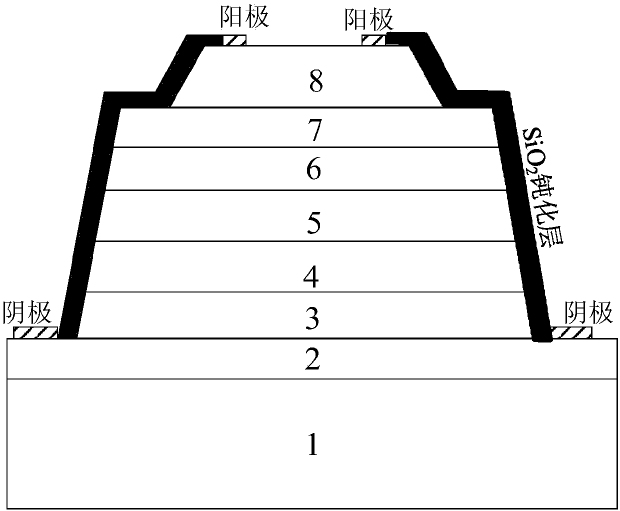
[0057] (1) Material structure growth. Using MOCVD to sequentially epitaxially grow a 1 μm thick N-InP buffer layer on an N-type heavily doped InP substrate with a doping concentration of 6.6×10 16 cm -3 ; 2 μm thick intrinsically doped In 0.53 Ga 0.47 As absorbing layer; 0.05μm thick N-In (1-x) Ga x As y P (1-y) Gradient composition layer, the doping concentration is 1×10 16 cm -3 ; 0.25 μm thick N-InP charge layer with a doping concentration of 1×10 17 cm -3 ; 0.5 μm thick intrinsically doped InP multiplication layer; 0.2 μm thick P-type doped InP electric field buffer layer with a doping concentration of 1×10 17 cm -3 ; 1 μm thick P-type heavily doped InP contact layer with a doping concentration of 1×10 19 cm -3 .

[0058] (2) Shallow mesa lithographic pattern transfer. The pattern on the photoresist plate is transferred to the photoresist through process steps such as gluing, exposure, and development.

[0059] (3) Shallow mesa etching. Using the photoresi...


PUM


Abstract

The invention belongs to the fields of photoelectric detection and image sensors, and in order to inhibit fringe field and reduce device dark current while guaranteeing a high field in the central area of the device, reference basis is provided for industrial application. The invention discloses a two-stage table-top InGaAs/InP avalanche photodiode and a preparation method thereof. The structure comprises an N<+>-InP substrate, an N-InP buffer layer, an N<->-InGaAs In0.53Ga0.47As absorbed layer, an N-InGaAsP In(1-x)GaxAsyP(1-y) component gradient layer, an N-InP charge layer, an i-InP multiplying layer, a P-InP field buffer layer and a P<+>-InP contact layer, wherein the P-InP field buffer layer forms a shallow table-top through etching, the N-InP buffer layer forms a deep table-top through etching, and constant impact ionization of photon-generated carriers inside the multiplying layer causes avalanche multiplication. The avalanche photodiode is mainly applied to the design occasionsof photoelectric detection and photoelectric sensors.

Description

technical field [0001] The invention belongs to the field of photoelectric detection and image sensors, and relates to a two-stage mesa InGaAs / InGaAs / InP avalanche photodiode and a preparation method thereof. Background technique [0002] In recent years, with the rise of big data carriers such as the Internet of Things, cloud computing, and mobile Internet, the amount of information transmission has increased in an avalanche. Challenges to data center network architecture. The development of traditional electrical interconnection is slow, and it is difficult to meet the requirements of high-performance processor interconnection communication. In contrast, optical interconnection uses photons as the information carrier, which has the advantages of low loss, fast speed and low delay, and can greatly increase the communication bandwidth density and effectively solve the interconnection bottleneck. Therefore, it is an inevitable trend of future interconnection. [0003] Optic...

Claims


Application Information

Patent Timeline
Patent Type & Authority Applications(China)
IPC IPC(8): H01L31/0352H01L31/107H01L31/18
CPCH01L31/035281H01L31/1075H01L31/18
Inventor 谢生朱帅宇毛陆虹
Owner TIANJIN UNIV
Why Eureka
Try Eureka