T type gate high electron mobility transistor (HEMT) device and manufacturing method thereof

A manufacturing method and device technology, applied in semiconductor/solid-state device manufacturing, semiconductor devices, electrical components, etc., can solve problems such as low breakdown voltage, achieve the effects of increased breakdown voltage, enhanced control capability, and reduced leakage voltage

Active Publication Date: 2015-06-10
昆山工研院第三代半导体研究院有限公司
View PDF3 Cites 0 Cited by
  • Summary
  • Abstract
  • Description
  • Claims
  • Application Information

AI Technical Summary

Problems solved by technology

[0009] In view of this, the present invention provides a T-gate HEMT device and a manufacturing method thereof to solve the problem of low breakdown voltage of the existing T-gate HEMT device

Method used


Image

  • T type gate high electron mobility transistor (HEMT) device and manufacturing method thereof
  • T type gate high electron mobility transistor (HEMT) device and manufacturing method thereof
  • T type gate high electron mobility transistor (HEMT) device and manufacturing method thereof

Examples


Embodiment 1

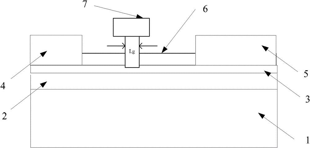
[0049] This embodiment discloses a method for manufacturing a T-shaped gate HEMT device, and the cross-sectional diagram of the device in each step is as follows Figure 2 to Figure 5 shown, including:

[0050] Step S1, providing a substrate.

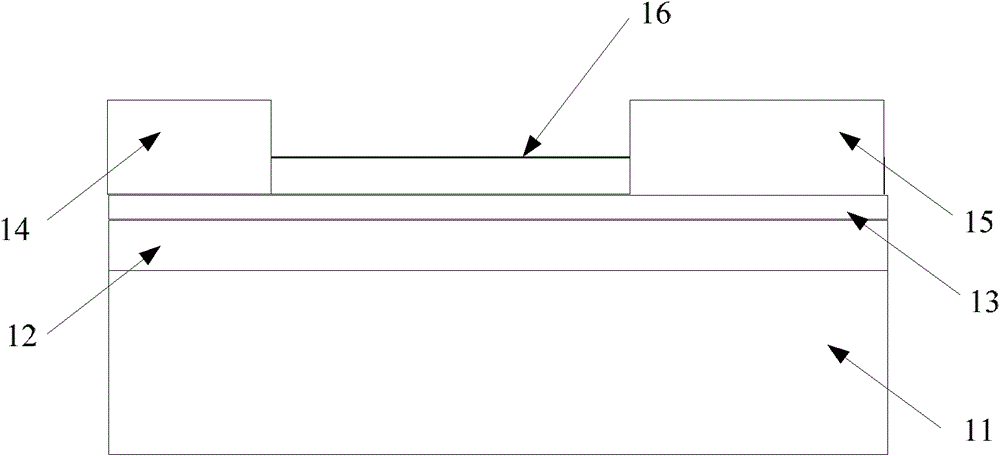
[0051] Such as figure 2 As shown, the base includes:

[0052] A body layer 11, the body layer 11 is preferably a silicon carbide layer;

[0053] A buffer layer 12 disposed on the surface of the body layer 11, the buffer layer 12 is a gallium nitride layer;

[0054] An epitaxial layer 13 disposed on the surface of the buffer layer 12, the epitaxial layer 13 is selected from an aluminum gallium nitride layer;

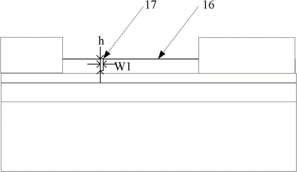
[0055] The source electrode 14, the drain electrode 15 and the passivation layer 16 between the source electrode 14 and the drain electrode 15 are arranged on the surface of the epitaxial layer 13, and the passivation layer 16 is a silicon nitride layer.

[0056] Specifically, the bandgap width of the material for making the ...

Embodiment 2

[0078] This embodiment discloses a T-gate HEMT device fabricated by the above embodiment, such as Figure 5 shown, the device includes:

[0079] The substrate, the substrate includes: a body layer 11, the body layer 11 is preferably a silicon carbide layer, a buffer layer 12 arranged on the surface of the body layer 11, the buffer layer 12 is a gallium nitride layer, and is arranged on the buffer layer The epitaxial layer 13 on the surface of the layer 12, the epitaxial layer 13 is selected as an aluminum gallium nitride layer, and the source 14, the drain 15 and the passivation between the source 14 and the drain 15 are arranged on the surface of the epitaxial layer 13. A layer 16, the passivation layer 16 is a silicon nitride layer;

[0080] T-shaped gate 21, the gate foot part of the T-shaped gate 21 penetrates the passivation layer 16 deep into the surface of the epitaxial layer 13, and the bottom of the gate foot is divided into two parts arranged in a ladder shape, Where...


PUM


Abstract

The invention discloses a T type gate high electron mobility transistor (HEMT) device and a manufacturing method thereof. The method comprises the following steps of: providing a substrate, wherein the substrate comprises a body layer, an epitaxial layer, a source, a drain and a passivation layer; forming a fine gate graph in the surface of the passivation layer; forming a dual-layer photoresist layer on the surface of the passivation layer with the fine gate graph, and forming a T type gate graph in the surface of the dual-layer photoresist layer; forming a gate pin graph of the T type gate graph in the surface of the passivation layer and the surface of the epitaxial layer; and forming a T type gate, wherein a gate pin of the T type gate passes through the passivation layer partially to penetrate into the surface of the epitaxial layer, the bottom of the gate pin is divided into two parts which are arranged in a step shape, and the part which is close to the source is longer than that which is close to the drain. An electric field generated by the T type gate is more uniform, and an edge electric field, which is close to one side of the drain, of the gate pin can be reduced during actual application, so that breakdown voltage of the device is boosted by reducing drain voltage.

Description

technical field [0001] The invention belongs to the field of semiconductor devices, in particular to a T-shaped gate HEMT device and a manufacturing method thereof. Background technique [0002] As the operating frequency of the HEMT (High Electron Mobility Transistors, high electron mobility transistor) device increases, the requirements for the cut-off frequency of the HEMT device also increase accordingly. [0003] The cut-off frequency of HEMT devices is an important factor to measure the high-speed performance of transistors, and its formula is: [0004] f T = v s 2 πL g , [0005] In the formula, v s is the saturation drift rate of carriers in the HEMT device, L g is the length of the gate in the HEMT device. [0006] Due to the saturation drift rate v of the carriers s is re...

Claims


Application Information

Patent Timeline
Patent Type & Authority Patents(China)
IPC IPC(8): H01L21/335H01L21/28H01L21/027H01L29/778H01L29/423
Inventor 魏珂刘新宇黄俊刘果果
Owner 昆山工研院第三代半导体研究院有限公司
Why Eureka
Try Eureka