

Delayed avalanche semiconductor device for inhibiting fringe electric field
A fringe electric field, semiconductor technology, applied in semiconductor devices, electrical components, circuits, etc., can solve the problems of short working life, increased cost, instability, etc. Effect
- Summary
- Abstract
- Description
- Claims
- Application Information
AI Technical Summary
Problems solved by technology
Method used
Image

Examples
Embodiment Construction
[0024] The present invention will be described in further detail below with reference to specific embodiments, but the embodiments of the present invention are not limited thereto.
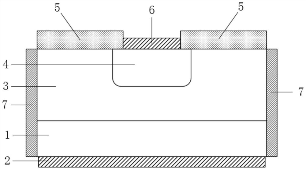
[0025] See figure 1 , a delayed avalanche semiconductor device for suppressing fringing electric field, comprising: N+ type substrate 1 , cathode 2 , P-drift region 3 , P+ active region 4 , oxide layer 5 , anode 6 and side electrode 7 .
[0026] The cathode 2, the N+ type substrate 1 and the P-drift region 3 are arranged in order from bottom to top.
[0027] The interface between the cathode 2 and the N+ type substrate 1 is an ohmic contact.
[0028] Ion implantation is performed on the P-drift region 3 to form a P+ active region 4 inside the P-drift region 3 .
[0029] The anode 6 is located above the P+ active region 4 , and the interface between the anode 6 and the P+ active region 4 is in ohmic contact; oxide layers 5 are respectively provided on both sides of the anode 6 .
[0030] The con...
PUM
 Abstract
Description
Claims
Application Information