

III-nitride semiconductor avalanche photodetector and preparation method thereof
A nitride semiconductor, avalanche photoelectric technology, applied in the field of photodetectors, can solve the problems of low composite dark current, high reliability and low fringing electric field on the surface of the device, so as to reduce the surface composite dark current, improve the reliability of the device, reduce the The effect of fringing electric fields
- Summary
- Abstract
- Description
- Claims
- Application Information
AI Technical Summary
Problems solved by technology
Method used
Image

Examples
Embodiment 1
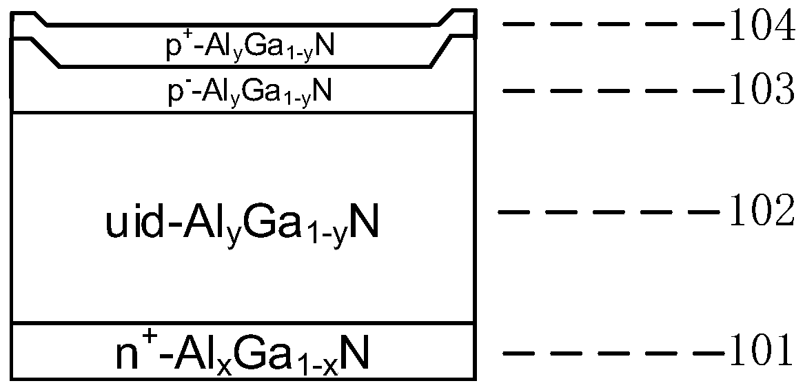
[0031] Such as figure 1 As shown, this embodiment provides a III-nitride semiconductor avalanche photodetector, specifically an AlGaN semiconductor avalanche photodetector based on a PIN structure, specifically including: 0.4 μm thick heavily doped n-type Al x Ga 1- x N ohmic contact layer 101, 160nm thick non-intentionally doped Al y Ga 1-y N layer 102 and a p-type layer with a thickness of 100nm; wherein, heavily doped n-type Al x Ga 1-x The Al composition x of the N ohmic contact layer 101 layer=0.6, and the electron concentration is 2×10 18 cm -3 , the unintentionally doped Al y Ga 1-y Al composition y=0.4 of N layer 102, electron concentration is 6×10 16 cm -3 .
[0032] Further, the p-type layer includes p-type Al with higher doping concentration sequentially stacked from top to bottom y Ga 1-y N layer 104, p-type Al with lower doping concentration y Ga 1-y N layer 103, the specific parameters are as follows:
[0033] (1) The n-type Al with low doping con...
Embodiment 2
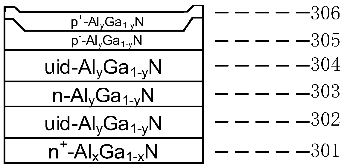
[0040] Such as image 3 As shown, this embodiment provides a III-nitride semiconductor avalanche photodetector, specifically, an AlGaN semiconductor avalanche photodetector based on a PININ absorption derived from a PIN structure and a multiplication separation structure, including: 0.4 μm thick heavily doped n-type Al x Ga 1-x N ohmic contact layer 301, 0.18 μm thick unintentionally doped Al y Ga 1-y N absorbing layer 302, 60nm thick Al y Ga 1-y N charge layer 303, 130nm thick unintentionally doped Al y Ga 1-y N multiplication layer 304 and a p-type layer with a thickness of 100nm; wherein, the Al composition x=0.6, y=0.4, and the heavily doped n-type Al x Ga 1-x The electron concentration of the N ohmic contact layer 301 is 2×10 18 cm -3 , the unintentionally doped Al y Ga 1-y The electron concentration of the N absorbing layer 302 is 6×10 16 cm -3 , the electron concentration of the charge layer 303 is 1×10 18 cm -3 , the electron concentration of the multip...
Embodiment 3
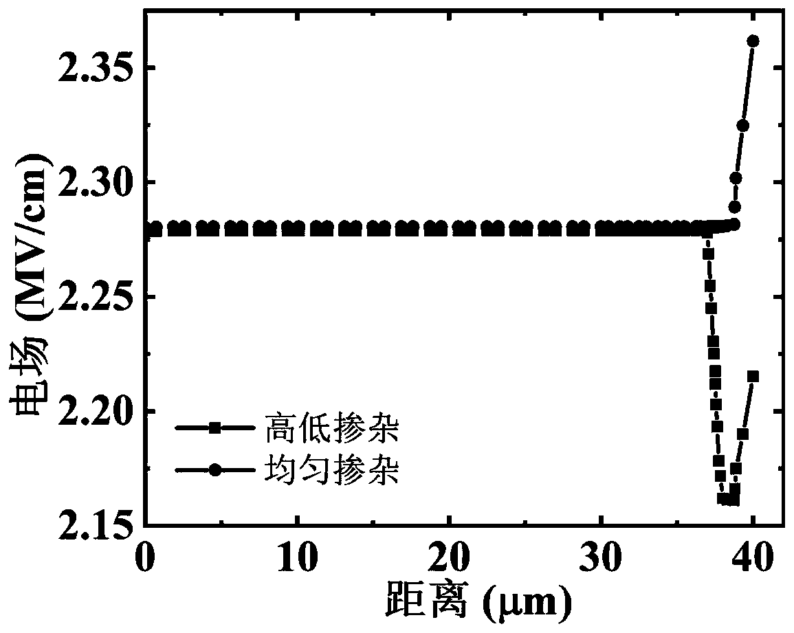
[0049] Such as Figure 4 As shown, the difference between this embodiment and embodiment 1 is that the p-type Al with higher doping concentration in the p-type layer y Ga 1-y The edge thickness of the N layer 104 is consistent with the thickness in the center of the device.
PUM
| Property | Measurement | Unit |
|---|---|---|
| Thickness | aaaaa | aaaaa |
| Thickness | aaaaa | aaaaa |
| Thickness | aaaaa | aaaaa |
Abstract
Description
Claims
Application Information