Side wall cavity layer structure of semiconductor device and method for preparing side wall cavity layer structure

A technology of semiconductor and layer structure, which is applied in the direction of semiconductor devices, semiconductor/solid-state device manufacturing, electrical components, etc., can solve the problems of enlargement and reduction of side wall thickness, and achieve the effect of simple structure and weakened gate potential. The effect of the method is simple and easy

Active Publication Date: 2015-01-07
SHANGHAI HUALI MICROELECTRONICS CORP
View PDF2 Cites 0 Cited by
  • Summary
  • Abstract
  • Description
  • Claims
  • Application Information

AI Technical Summary

Problems solved by technology

At the same time, as the size of the device continues to decrease, the thickness of the sidewall also decreases. At this time, the effect of the contact hole on the gate potential through the capacitive coupling of the sidewall will become larger.

Method used


Image

  • Side wall cavity layer structure of semiconductor device and method for preparing side wall cavity layer structure
  • Side wall cavity layer structure of semiconductor device and method for preparing side wall cavity layer structure
  • Side wall cavity layer structure of semiconductor device and method for preparing side wall cavity layer structure

Examples


Embodiment Construction

[0029] The present invention will be explained in detail below in conjunction with the accompanying drawings.

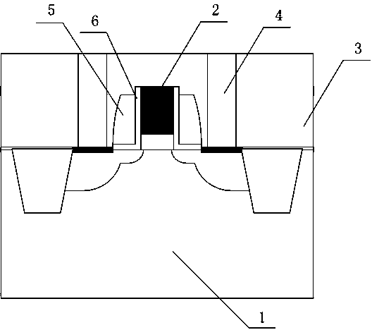
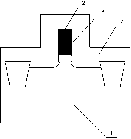
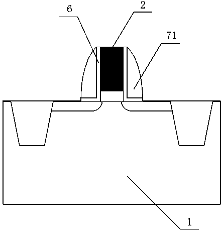
[0030] Such as figure 1 A sidewall cavity layer structure of a semiconductor device according to an embodiment of the present invention shown in , includes a semiconductor substrate 1 , a gate 2 , a dielectric layer 3 and a contact hole 4 . The outer side of the gate 2 is provided with a void layer 5, and between the void layer 5 and the gate 2 and the semiconductor substrate 1 is provided with SiO 2 Layer 6.

[0031] The present invention effectively reduces the dielectric constant of the sidewall material by introducing a void layer in the sidewall, thereby weakening the effect that the fringe electric field of the source and drain of the device affects the channel through the capacitive coupling of the sidewall and the capacitive coupling of the contact hole through the sidewall Effects on the gate potential.

[0032] In an embodiment of the present invention, ...


PUM


Abstract

The invention provides a side wall cavity layer structure of a semiconductor device, which comprises a semiconductor substrate, a grid electrode, a dielectric layer and a contact hole. Cavity layers are disposed on two sides of the grid electrode, and SiO2 layers are disposed between each cavity layer and the grid electrode and between each cavity layer and the semiconductor substrate. The invention further provides a method for preparing the side wall cavity layer structure of the semiconductor device. The method includes steps: depositing an amorphous carbon layer on the semiconductor substrate with the grid electrode and forming amorphous carbon side walls by means of self-alignment etching; chemically and mechanically grinding the dielectric layer until the amorphous carbon side walls are exposed, then carrying out ashing treatment to completely ash and clean the amorphous carbon side walls, and continuing ashing until a SiO2 layer is formed on the grid electrode and an exposed silicon surface; and quickly filling the dielectric layer so that holes are kept on portions without the amorphous carbon side walls. The side wall cavity layer structure of the semiconductor device is simple, and the method is simple, convenient and feasible.

Description

technical field [0001] The invention belongs to the field of semiconductor technology, and relates to a semiconductor device sidewall structure and a preparation method thereof, in particular to a semiconductor device sidewall cavity layer structure and a preparation method thereof. Background technique [0002] Short Channel Effect (Short Channel Effect) is a common phenomenon when the channel length of CMOS devices is reduced. Press down) and other characteristics, in severe cases, it will cause the performance of CMOS devices to fail. [0003] The principle can be explained by the charge sharing model, that is, when the channel becomes shorter, the ratio of the charge in the channel depletion region shared by the source liner and the drain liner PN junction to the total charge in the channel will increase, resulting in a decrease in gate control capability. [0004] However, the traditional charge sharing model does not take into account the effect of the fringe electric...

Claims


Application Information

Patent Timeline
Patent Type & Authority Patents(China)
IPC IPC(8): H01L29/78H01L21/336
Inventor 黄晓橹周军
Owner SHANGHAI HUALI MICROELECTRONICS CORP
Why Eureka
Try Eureka