Low-leakage-current schottky diode

A Schottky diode and leakage current technology, applied in circuits, electrical components, semiconductor devices, etc., can solve problems such as increased reverse leakage current, large reverse leakage current, uneven local current distribution, etc., and achieve edge electric field Reduce, reduce the reverse leakage current, improve the effect of uniformity

Inactive Publication Date: 2017-05-17
杭州易正科技有限公司
View PDF4 Cites 0 Cited by
  • Summary
  • Abstract
  • Description
  • Claims
  • Application Information

AI Technical Summary

Problems solved by technology

Schottky diodes can provide greater forward current work faster than general PN junction diodes, but their reverse leakage current is also large. At the same time, due to junction curvature and other local strong electric fields at the edge, resulting in uneven local current distribution, Its reverse leakage current increases, which affects the further expansion of its application

Method used


Image

  • Low-leakage-current schottky diode
  • Low-leakage-current schottky diode
  • Low-leakage-current schottky diode

Examples


no. 1 example

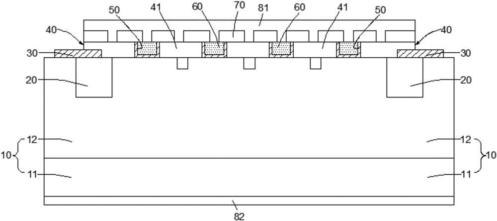
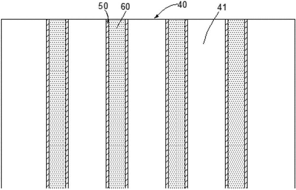
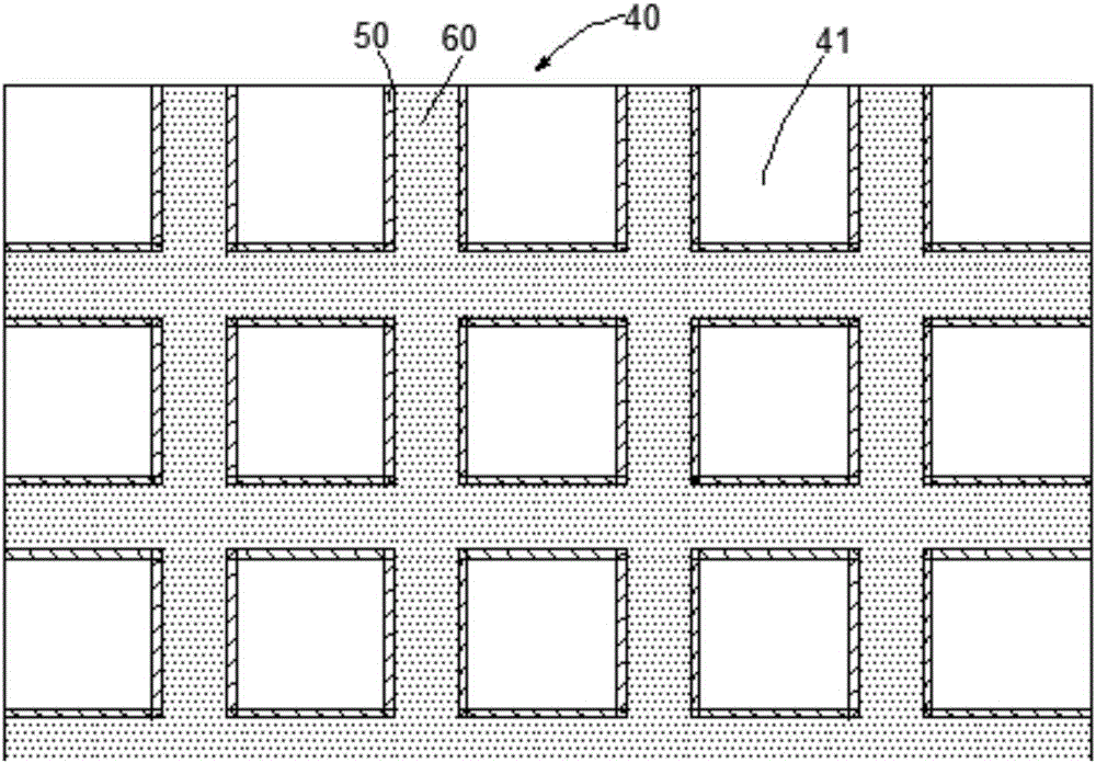
[0025] Such as figure 1 As shown, the Schottky diode with low leakage current in this embodiment includes: a first conductivity type semiconductor substrate 10, a second conductivity type protection area 20 formed in the upper surface layer on both sides of the first conductivity type semiconductor substrate 10, The insulating layer 30 formed on the second conductivity type protection region 20, the barrier metal layer 40 formed on the first conductivity type semiconductor substrate 10 and the second conductivity type protection region 20, the barrier metal layer 40 and the The insulating layers 30 are connected, and the barrier metal layer 40 is composed of a plurality of discontinuous electrically connected barrier metal layers 41. Adjacent barrier metal layers 41 are separated by insulating grooves 50, and the insulating grooves The groove 50 is filled with a conductive medium 60 , and the conductive medium 60 is electrically connected to the barrier metal layer 40 .

[00...

no. 2 example

[0031] Such as figure 2 As shown, in this embodiment, on the basis of the technical solution of the first embodiment, a doped region 90 of the second conductivity type is formed under the center of the barrier metal layer 41, and the doped region 90 of the second conductivity type is connected to the doped region of the first conductivity type. Type lightly doped layer 12 forms a PN junction, under the reverse voltage, assists the depletion layer of the gate structure formed by the insulating groove 50 and the conductive medium 60, and the two work together to further reduce the reverse leakage current.


PUM


Abstract

The invention relates to the technical field of a semiconductor, particularly to a low-leakage-current schottky diode. The low-leakage-current schottky diode comprises first conductive type semiconductor substrates, second conductive type protection regions formed on the upper surface layers on the two sides of the first conductive type semiconductor substrates, insulating layers formed on the second conductive type protection regions, barrier metal layers formed on the first conductive type substrates and the second conductive type protection regions, wherein the barrier metal layers are connected with the insulating layers; each barrier metal layer consists of a plurality of discontinuous electrically-connected barrier metal sub layers; the adjacent barrier metal sub layers are isolated by an insulating groove; each insulating groove is filled with a conducting medium; and the conducting medium is electrically connected with the barrier metal layers.

Description

technical field [0001] The invention relates to the technical field of semiconductors, in particular to a Schottky diode with low leakage current. [0002] technical background [0003] A Schottky barrier diode is a semiconductor element in which a semiconductor layer and a metal layer are connected through a Schottky junction, and the rectification function of the Schottky barrier is utilized. Schottky diodes have the advantages of low power, high current and ultra-high speed, and are favored in the field of electronic devices. Schottky diodes can provide greater forward current work faster than general PN junction diodes, but their reverse leakage current is also large. At the same time, due to junction curvature and other local strong electric fields at the edge, resulting in uneven local current distribution, Its reverse leakage current increases, which affects the further expansion of its application. Contents of the invention [0004] The object of the present inven...

Claims


Application Information

Patent Timeline
Patent Type & Authority Applications(China)
IPC IPC(8): H01L29/06H01L29/872
CPCH01L29/0607H01L29/872
Inventor 李风浪
Owner 杭州易正科技有限公司
Why Eureka
Try Eureka