Organic/inorganic hybrid optical amplifier with wavelength conversion

an organic/inorganic hybrid, optical amplifier technology, applied in the field of optical amplifiers, can solve the problems of high cost, complicated manufacturing of arrays, and general cost, and achieve the effect of improving absorption and emission efficiency

Active Publication Date: 2013-08-22
BAN DAYAN +2
View PDF31 Cites 21 Cited by
  • Summary
  • Abstract
  • Description
  • Claims
  • Application Information

AI Technical Summary

Benefits of technology

[0028]FIG. 4(a) is a schematic cross-section of a hybrid optical up-converter device of the present invention, with integrated InGaAs/InP HPT and an OLED. Note that the thickness of the org

Problems solved by technology

Such arrays are generally complicated to manufacture and costly.
The above methods a

Method used


Image

  • Organic/inorganic hybrid optical amplifier with wavelength conversion
  • Organic/inorganic hybrid optical amplifier with wavelength conversion
  • Organic/inorganic hybrid optical amplifier with wavelength conversion

Examples


examples of implementation

of the Invention

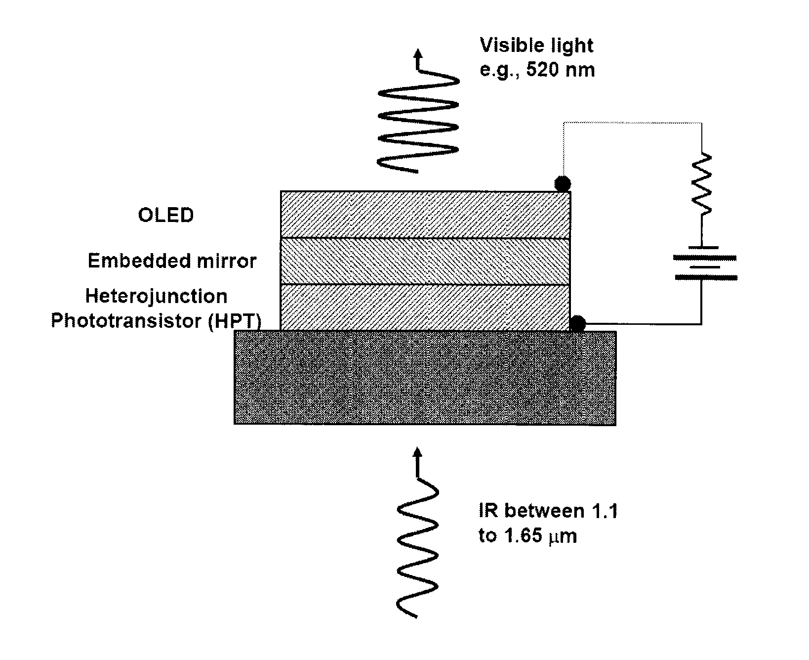
[0045]In another aspect of the invention, the integration of the components or portions as described may be provided by means of direct tandem integration of an MOCVD-grown In0.53Ga0.47As / InP p-n-p HPT layers, a thin Au layer, and organic light emitting diode layers on a single InP substrate.

[0046]It should be understood that the operation of an In0.53Ga0.47As / InP based HPT is similar to that of a typical bipolar junction transistor, and is well known in the art, for example Chapter 7 of “Solid State Electronic Devices”, 6th edition, by Streetman and Banerjee. The InGaAs based HPT generally responds to visible and infrared light over a wavelength range from 0.9 to 1.65 μm. A representative HPT structure suitable for use in the structure of the present invention may consist of a p-doped InGaAs collector layer, a n-doped InGaAs base layer, and a p-doped InP emitter layer. This p-n-p structure is biased with a forward-biased emitter junction and a reverse-biased collect...


PUM


Abstract

A device and related fabrication method is provided for an organic/inorganic hybrid optical amplifier with a function of converting infrared light to visible light. The hybrid device integrates an inorganic heterojunction phototransistor (HPT), an embedded metal electrode mirror with a dual function as an optical mirror and charge injection electrode, and an organic light emitting diode (OLED). This integrated optical amplifier is capable of amplifying the incoming light and producing light emission with a power greater than that of the incoming signal. In the second aspect of the invention, the optical amplifier is capable of detecting an incoming infrared electromagnetic wave and converting the wave back to a visible light wave. The optical device has dual functions of optical power amplification and photon energy up-conversion. The optical amplifier device consists of an InGaAs/InP based HPT structure as photodetector, gold-coated metals as embedded mirror and a top-emission OLED. New optical up-conversion imaging devices are also provided that include focal-point array of the organic/inorganic hybrid optical amplifier devices in pixelated formats. The up-conversion imaging devices have a fast response time to enable gated operation for practical applications such as night vision, active surveillance, semiconductor wafer inspection and eye-safe infrared imaging. More importantly, the up-conversion imaging devices would be particularly useful for detecting ultra-low intensity infrared scenes.

Description

FIELD OF THE INVENTION[0001]The invention relates generally to the field of optical amplifiers. This invention further relates to devices that incorporate infrared imaging.BACKGROUND OF THE INVENTION[0002]Infrared imaging is widely used in a variety of applications including night vision, surveillance, search and rescue, remote sensing, and preventive maintenance. Imaging devices to provide these applications are typically constructed of HgCdTe or InSb focal plane arrays. For example, quantum well infrared photodetectors (QWIPs) can detect mid- and far-infrared light, and are operable to generate an output current from the light source. Such arrays are generally complicated to manufacture and costly.[0003]Infrared thermal imaging, which incorporates GaAs QWIPs and GaAs light emitting diodes (LEDs) via monolithic epitaxial growth integration, was disclosed by one of the applicants, H. C. Liu, in U.S. Pat. No. 5,567,955 issued Oct. 22, 1996 to the National Research Council of Canada, ...

Claims


Application Information

Patent Timeline
IPC IPC(8): H01L31/14
CPCH01L27/3227H01L31/153H01L2251/5315G02F1/015H01L31/14G02F2202/102G02F2202/12G02F2203/11G02F2202/101H10K59/60H10K2102/3026
Inventor BAN, DAYANLU, ZHENGHONGCHEN, JUN
Owner BAN DAYAN
Why Eureka
Try Eureka