Organic light emitting device

a light-emitting device and organic technology, applied in the field of display devices, can solve the problems of imperfect sealing process and easy degradation of organic light-emitting devices, and achieve the effect of increasing life and reliability

Active Publication Date: 2010-01-26
LG ELECTRONICS INC
View PDF3 Cites 26 Cited by
  • Summary
  • Abstract
  • Description
  • Claims
  • Application Information

AI Technical Summary

Benefits of technology

[0010]An exemplary embodiment provides an organic light emitting device capable of increasing life span and reliability.

Problems solved by technology

However, the organic light emitting device may be easily degraded by an inner factor such as a degradation of a cathode electrode due to oxygen, a degradation of a reaction between the light emitting layer and an interface, and an external factor such as moisture, oxygen, ultraviolet rays, and product conditions.
In particular, since moisture and oxygen permeated from outside have fatal influence on life span of the organic light emitting device, a sealing process in the organic light emitting device is very important.
In case of the organic light emitting device using a flexible substrate such as stainless steel or plastic film which has been recently developed, a sealing process is not perfect.

Method used


Image

  • Organic light emitting device
  • Organic light emitting device
  • Organic light emitting device

Examples


Embodiment Construction

[0025]Reference will now be made in detail embodiments of the invention examples of which are illustrated in the accompanying drawings.

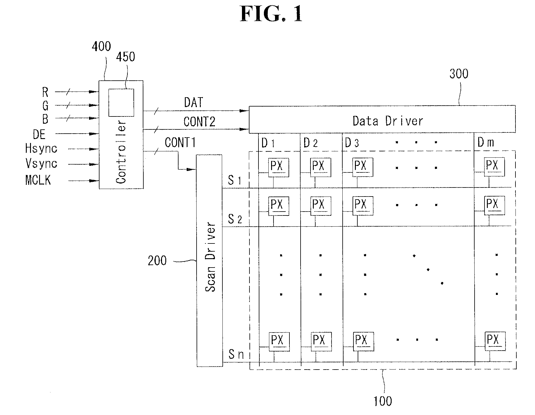
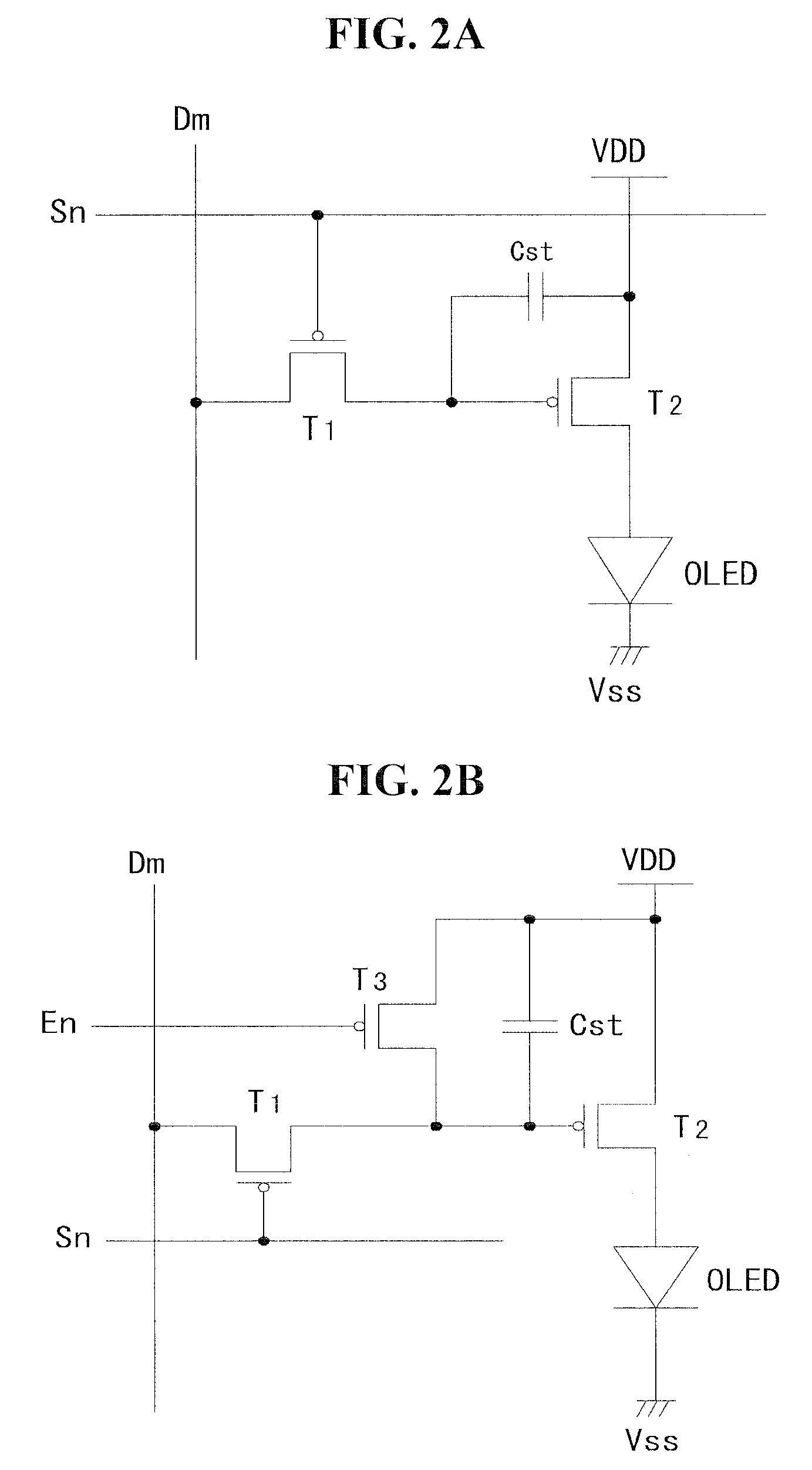
[0026]FIG. 1 is a bock diagram of an organic light emitting device according to an exemplary embodiment, and FIGS. 2A and 2B are circuit diagrams of a subpixel of the organic light emitting device.

[0027]As shown in FIG. 1, the organic light emitting device according to the exemplary embodiment includes a display panel 100, a scan driver 200, a data driver 300, and a controller 400.

[0028]The display panel 100 includes a plurality of signal lines S1 to Sn and D1 to Dm, a plurality of power supply lines (not shown), and a plurality of subpixels PX arranged in a matrix format to be connected to the signal lines S1 to Sn and D1 to Dm and the power supply lines.

[0029]The plurality of signal lines S1 to Sn and D1 to Dm may include the plurality of scan lines S1 to Sn for transmitting scan signals and the plurality of data lines D1 to Dm for transmitting dat...


PUM


Abstract

An organic light emitting device is disclosed. The organic light emitting device includes a first substrate, a display unit that is positioned on the first substrate and includes a plurality of subpixels, a second substrate facing the first substrate, a seal member attaching the first substrate to the second substrate, and at least one projection. The seal member substantially has a water vapor permeation rate of 100 g / m2 day to 103 g / m2 day. The projection is positioned at a location corresponding to a bezel area of at least one of the first and second substrates.

Description

[0001]This application claims the benefit of Korean Patent Application No. 10-2007-0063073 filed on Jun. 26, 2007, which is hereby incorporated by reference.BACKGROUND[0002]1. Field[0003]An exemplary embodiment relates to a display device, and more particularly, to an organic light emitting device.[0004]2. Description of the Related Art[0005]An organic light emitting device is a self-emitting device including a light emitting layer between two electrodes.[0006]The organic light emitting device may have a top emission structure and a bottom emission structure depending on an emission direction of light. The organic light emitting device may be classified into a passive matrix type organic light emitting device and an active matrix type organic light emitting device depending on a driving manner.[0007]However, the organic light emitting device may be easily degraded by an inner factor such as a degradation of a cathode electrode due to oxygen, a degradation of a reaction between the l...

Claims


Application Information

Patent Timeline
Patent Type & Authority Patents(United States)
IPC IPC(8): H05B33/00
CPCH01L51/5246H01L51/5253H01L51/524H01L51/5259H01L51/56H10K50/841H10K50/8426H10K50/846H10K50/844H10K71/00H05B33/04
Inventor PARK, SANGTAEKIM, MYUNGSEOPSEO, JEONGDAEYANG, WONJAECHOI, HYUNJUSHIN, YOUNGHOONHYEON, CHANGHOLEE, JONGMOO
Owner LG ELECTRONICS INC
Why Eureka
Try Eureka