Optical element, method for manufacturing optical element, and semi-transmissive semi-reflective liquid crystal display device

a liquid crystal display device and optical element technology, applied in the direction of liquid crystal compositions, instruments, chemistry apparatuses and processes, etc., can solve the problems of complex manufacturing process and reduced light utilization efficiency, and achieve the effect of reducing light utilization efficiency, simplifying device configuration, and reducing the thickness of the liquid crystal display devi

Inactive Publication Date: 2010-01-26
DAI NIPPON PRINTING CO LTD
View PDF6 Cites 0 Cited by
  • Summary
  • Abstract
  • Description
  • Claims
  • Application Information

AI Technical Summary

Benefits of technology

[0051]With the optical element in accordance with the present invention, it is possible to generate a phase difference between the light prior to passing through the optical element and the light that was transmitted through the optical element in the liquid crystal phase sections and to generate practically no phase difference between the light prior to passing through the optical element and the light that was transmitted through the optical element in the isotropic phase sections. Furthermore, with such optical element, the isotropic phase sections that have liquid crystals of isotropic phase and liquid crystal phase sections that have liquid crystals of liquid crystal phase and are adjacent to the isotropic phase sections are formed and zones where the phase difference is generated according to a predetermined pattern and zones where no phase difference is generated can be formed according to the transmission positions of the light irradiated on the optical element.
[0060]In addition, with the liquid crystal display device in accordance with the present invention, when transmissive display is performed, it is not necessary that the light from the light source irradiated toward the liquid crystal layer be transmitted through the ¼ wavelength plate. Therefore, the above-described problem associated with the decrease in the light utilization efficiency can be resolved.

Problems solved by technology

The resultant problem is that the light utilization efficiency is decreased.
Thus, the steps of forming and etching the photosensitive resin layer are required in the manufacture of the liquid crystal display device and the manufacturing process is complex.

Method used


Image

  • Optical element, method for manufacturing optical element, and semi-transmissive semi-reflective liquid crystal display device
  • Optical element, method for manufacturing optical element, and semi-transmissive semi-reflective liquid crystal display device
  • Optical element, method for manufacturing optical element, and semi-transmissive semi-reflective liquid crystal display device

Examples


example 1

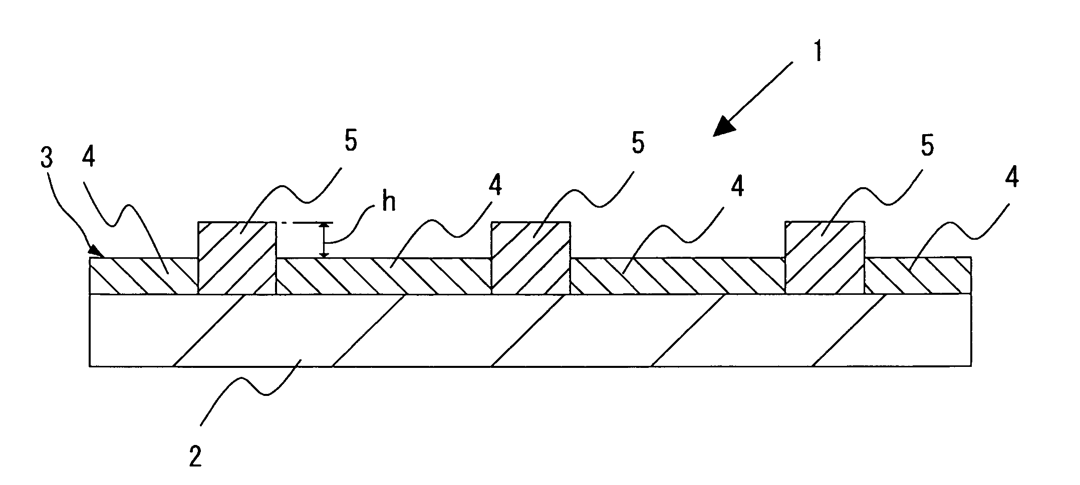
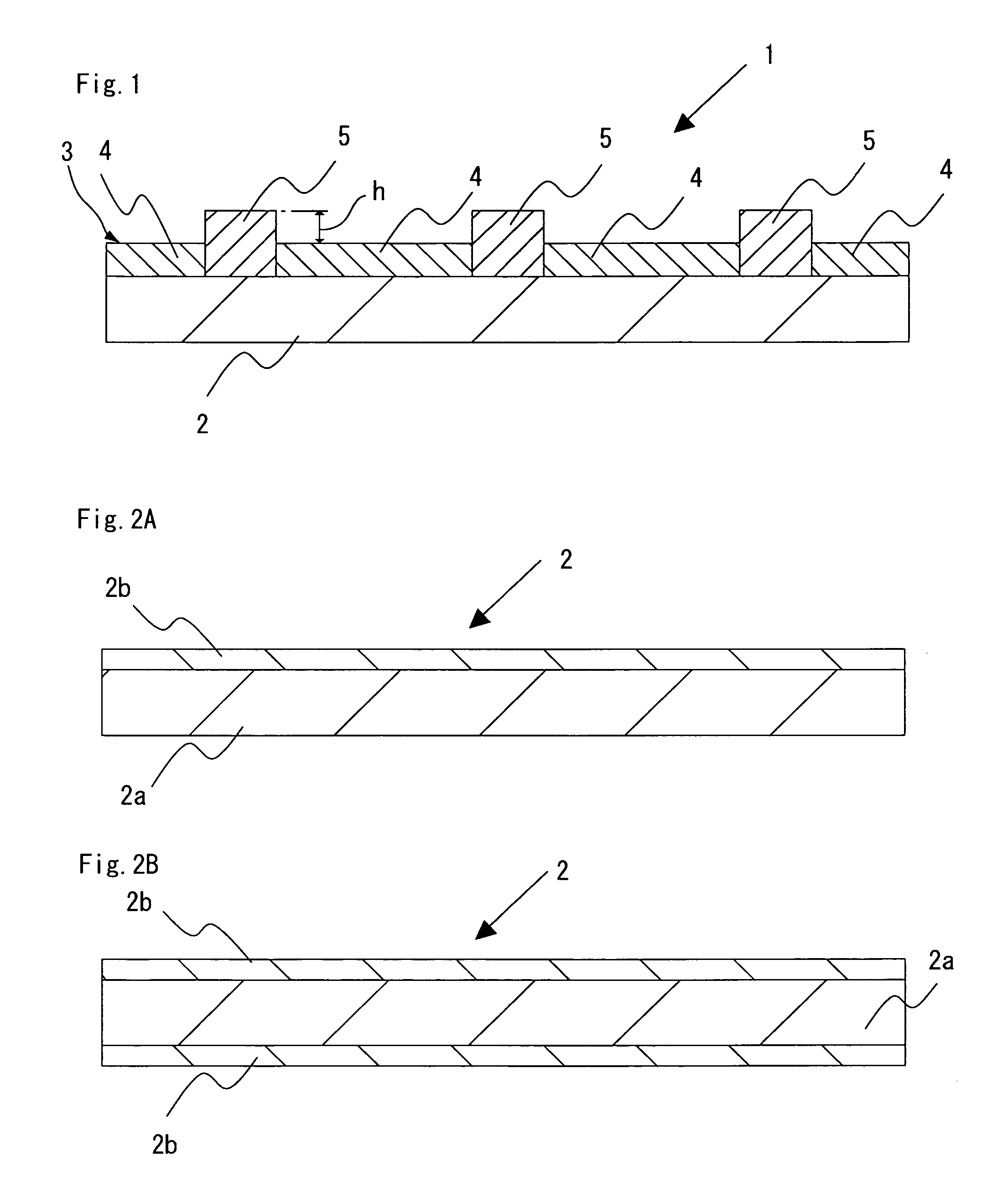
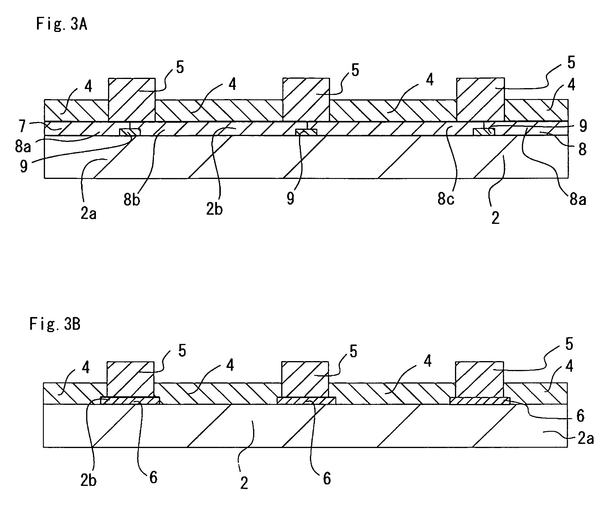
[0247]A substrate was prepared by successively laminating a color layer and an oriented film on a substrate main section as described hereinbelow, and an optical element was obtained by using such substrate.

Preparation of Coloration Material Dispersions for Formation of Color Layer

[0248]Pigment dispersion-type photoresists were used as coloration material dispersions for black matrix (BM) and color pixels of red (R), green (G), and blue (B). The pigment dispersion-type photoresist was obtained by using a pigment as a coloration material, adding beads to a dispersion composition (comprised a pigment, a dispersant, and a solvent), dispersing for 3 h in a dispersing apparatus, removing the beads, and mixing the dispersion thus obtained with a clear resist composition (comprised a polymer, a monomer, an additive, an initiator, and a solvent). The pigment dispersion-type photoresists had the following compositions in the case of using for forming reflective display sections in the RGB co...

example 2

[0364]An optical element was obtained in the same manner as in Example 1, except that the exposure dose during formation of the liquid crystal phase sections was 400 mJ / cm2. The liquid crystal phase section protrusion height of the liquid crystal phase sections and isotropic phase sections in the optical element thus obtained was as shown in Table 1. A liquid crystal display device was then fabricated in the same manner as in Example 1, except that the height of columns during processing conducted to form the color filters by using the optical element thus obtained, was 2.2 μm, and the TN liquid crystal used for forming the cell was ZLI-2293 (Δn=0.1332) manufactured by Merck Co., Ltd. The transmission factor and reflection factor of the liquid crystal display device were measured. The results are shown in Table 1.


PUM

PropertyMeasurementUnit
thicknessaaaaaaaaaa
thicknessaaaaaaaaaa
wavelengthaaaaaaaaaa

Abstract

The optical element in accordance with the present invention comprises a substrate having a light transmission ability and a fixed liquid crystal layer formed on the substrate. The fixed liquid crystal layer is composed of liquid crystal phase sections in which a liquid crystalline compound is fixed in a liquid crystal phase state and isotropic phase sections in which a liquid crystalline compound is fixed in an isotropic phase state.The layer thickness of the liquid crystal phase sections is larger than that of the isotropic phase sections, and the liquid crystal phase sections are formed so as to protrude with respect to the isotropic phase sections.

Description

BACKGROUND OF THE INVENTION[0001]1. Field of the Invention[0002]The present invention relates to an optical element for imparting a phase difference (retardation) to the light transmitted therethrough and to a method for manufacturing same, and more particularly to an optical element to be incorporated in a semi-transmissive semi-reflective liquid crystal display device to provide a phase difference suitable for transmissive display or reflective display and to a method for manufacturing such optical element. Furthermore, the present invention also relates to a semi-transmissive semi-reflective liquid crystal display device incorporating such optical element.[0003]2. Description of the Related Art[0004]A liquid crystal display device has been suggested that combines the function of a reflective liquid crystal display device in which the light introduced into the liquid crystal display device from the outside (external light) is reflected by a reflection plate and passed through a li...

Claims


Application Information

Patent Timeline
Patent Type & Authority Patents(United States)
IPC IPC(8): C09K19/02
CPCC09K19/02C09K19/2007G02F1/07G02F1/133555G02F1/133371G02F2413/09G02F1/133631
Inventor HAYASHI, SHINJIMORIYA, NORIHISA
Owner DAI NIPPON PRINTING CO LTD
Why Eureka
Try Eureka