
Method for using transitional voltage during programming of non-volatile storage

a technology of transitional voltage and programming method, applied in the field of non-volatile storage, can solve problems such as the programming of selected non-volatile storage elements, and achieve the effect of reducing program disturban

Active Publication Date: 2010-02-02
SANDISK TECH LLC
View PDF7 Cites 12 Cited by
  • Summary
  • Abstract
  • Description
  • Claims
  • Application Information

AI Technical Summary

Benefits of technology

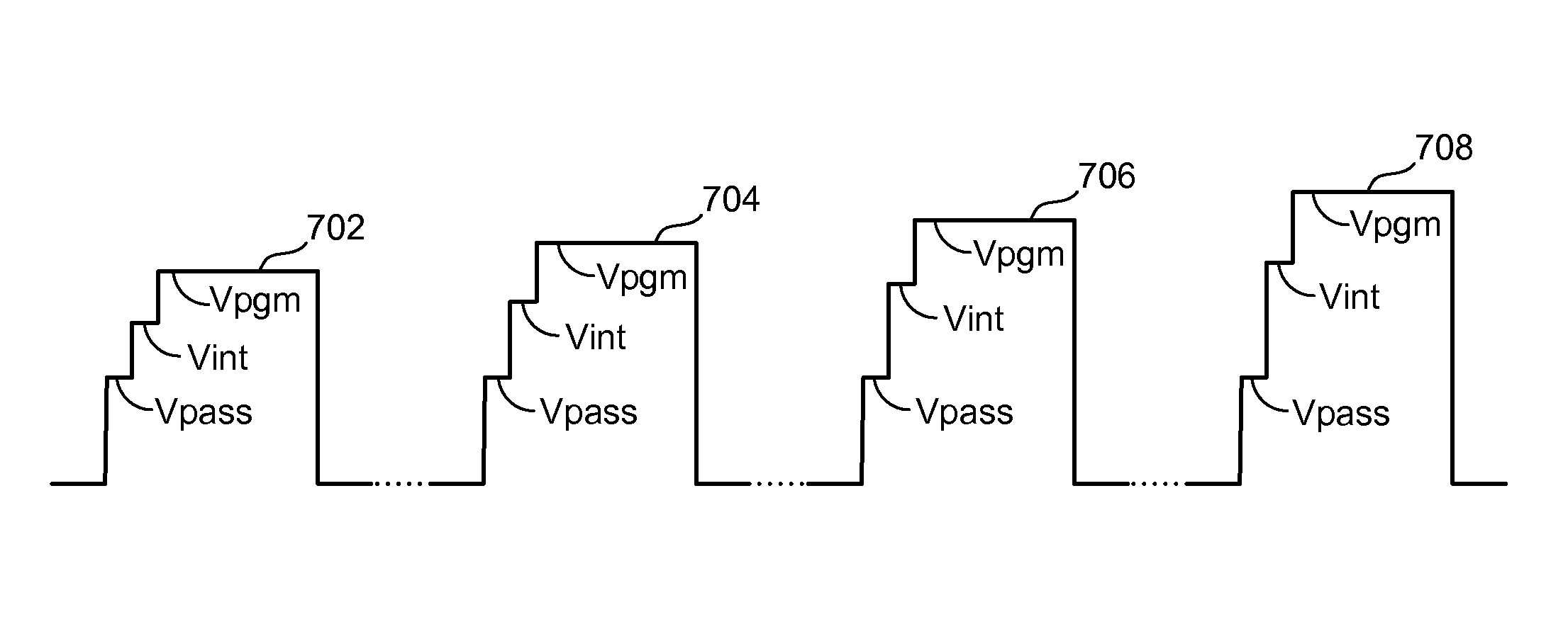
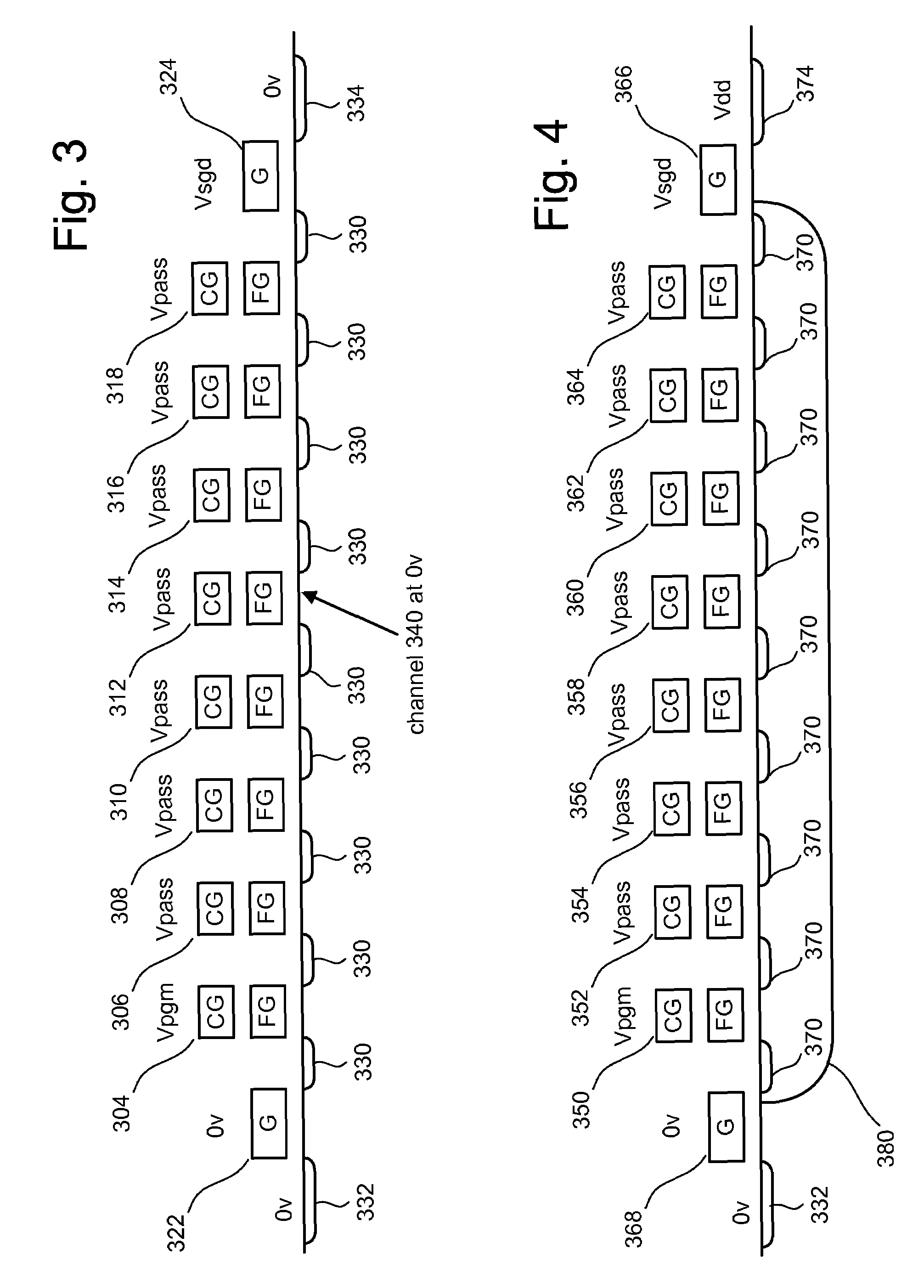
The technology described in this patent reduces program disturb in non-volatile storage elements by applying a programming signal in two stages. The first stage involves ramping up to a higher voltage before the programming signal is applied to the selected memory cell. This higher voltage is lower than the programming voltage, but it can still cause some current to flow. The second stage involves applying the programming signal to the selected cell and other unselected cells, while keeping the first stage voltage constant. This second stage programming signal is higher than the first stage, but it is not large enough to cause programming of the selected cell. By applying these two stages of programming, the technology reduces program disturb and improves the reliability of non-volatile storage elements.

Problems solved by technology

The first magnitude is not large enough to intentionally cause programming of the selected non-volatile storage element.
The first intermediate magnitude is not large enough to intentionally cause programming of the selected non-volatile storage element.
The second intermediate magnitude is not large enough to cause intentionally programming of the selected non-volatile storage element.

Method used


Image

  • Method for using transitional voltage during programming of non-volatile storage
  • Method for using transitional voltage during programming of non-volatile storage
  • Method for using transitional voltage during programming of non-volatile storage

Examples


Embodiment Construction

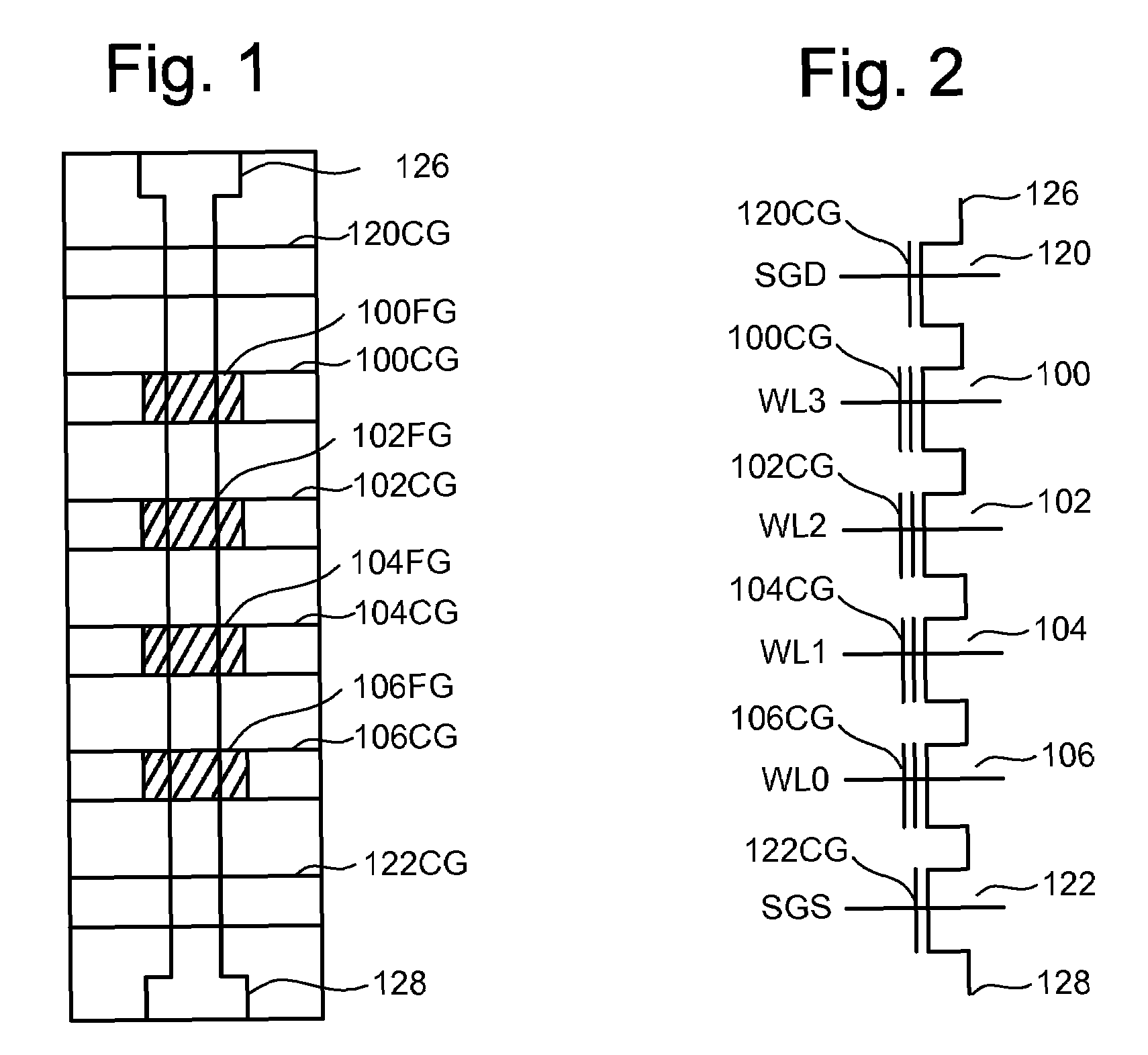
[0053]One example of a memory system suitable for implementing the present invention uses the NAND flash memory structure. However, other types of non-volatile storage devices can also be used.

[0054]FIG. 6 illustrates a memory device 396 having read / write circuits for reading and programming a page of memory cells in parallel, according to one embodiment. Memory device 396 may include one or more memory die 398. Memory die 398 includes a two-dimensional array of memory cells 400, control circuitry 410, and read / write circuits 465. In some embodiments, the array of memory cells can be three dimensional. Memory array 400 is addressable by word lines via row decoder 430 and by bit lines via column decoder 460. Read / write circuits 465 include multiple sense blocks 500 and allow a page of memory cells to be read or programmed in parallel. A controller 450 can be included in the same memory device 396 (e.g., a removable storage card) as the one or more memory die 398. Commands and Data ar...


PUM


Abstract

To program one or more non-volatile storage elements, a set of programming pulses are applied to at least one selected non-volatile storage element and one or more particular unselected non-volatile storage elements, for example, via a common word line. A boosting voltage is applied to other unselected non-volatile storage elements during the programming process in order to boost the channels of the unselected non-volatile storage elements so that programming will be inhibited. Each of the programming pulses has a first intermediate magnitude, a second intermediate magnitude and a third magnitude. In one embodiment, the first intermediate magnitude is similar to or the same as the boosting voltage. The second intermediate magnitude is greater than the first intermediate magnitude, but less then the third magnitude. Such an arrangement can reduce the effects of program disturb.

Description

CROSS-REFERENCE TO RELATED APPLICATIONS[0001]The following application is cross-referenced and incorporated by reference herein in its entirety: U.S. patent application Ser. No. 11 / 753,963 entitled “Non-Volatile Storage System With Transitional Voltage During Programming,” by Yinga Dong, Jeffrey W. Lutze and Dana Lee, filed the same day as the present application.BACKGROUND OF THE INVENTION[0002]1. Field of the Invention[0003]The present invention relates to technology for non-volatile storage.[0004]2. Description of the Related Art[0005]Semiconductor memory devices have become more popular for use in various electronic devices. For example, non-volatile semiconductor memory is used in cellular telephones, digital cameras, personal digital assistants, mobile computing devices, non-mobile computing devices and other devices. Electrical Erasable Programmable Read Only Memory (EEPROM) and flash memory are among the most popular non-volatile semiconductor memories.[0006]Many types of EE...

Claims


Application Information

Patent Timeline
Patent Type & Authority Patents(United States)
IPC IPC(8): G11C16/04
CPCG11C16/0483G11C16/10G11C16/12
Inventor DONG, YINGDALUTZE, JEFFREY W.LEE, DANA
Owner SANDISK TECH LLC
Learn More