Content addresable memory having selectively interconnected counter circuits

a counter circuit and addresable memory technology, applied in the field of content addressable memory (cam) devices, can solve the problems of unutilized memory area, cam system of '715 patent will not always output the correct match address, and inability to use the memory area

Inactive Publication Date: 2010-02-09
AVAGO TECH WIRELESS IP SINGAPORE PTE
View PDF15 Cites 58 Cited by
  • Summary
  • Abstract
  • Description
  • Claims
  • Application Information

AI Technical Summary

Problems solved by technology

It appears, however, that the CAM system of the '715 patent will not always output the correct match address.
Additionally, it appears that the CAM system of the '715 patent will not always function correctly when each data line has different numbers of data words.
Unfortunately, because the WEL in a CAM row can combine the row's match state only with the match state of an adjacent CAM row to generate an output match signal, and then can route the row's output match signal to only another adjacent CAM row, the row output match states can only be shifted sequentially across the array one row at a time.
Further, because data word chains must be stored in contiguous rows of the '789 CAM array, there may be many available (e.g., un-occupied) rows scattered across the array that cannot be used to store data word chains because the available rows are not contiguous, thereby resulting in unutilized memory area.
Unfortunately, table management tools that re-arrange able contents are burdensome and time consuming.
Further, because match signals from a CAM row in the '789 patent can be routed to only one adjacent row at a time, it is not feasible to store large numbers of regular expressions in the CAM device of the '789 patent.

Method used


Image

  • Content addresable memory having selectively interconnected counter circuits
  • Content addresable memory having selectively interconnected counter circuits
  • Content addresable memory having selectively interconnected counter circuits

Examples


Embodiment Construction

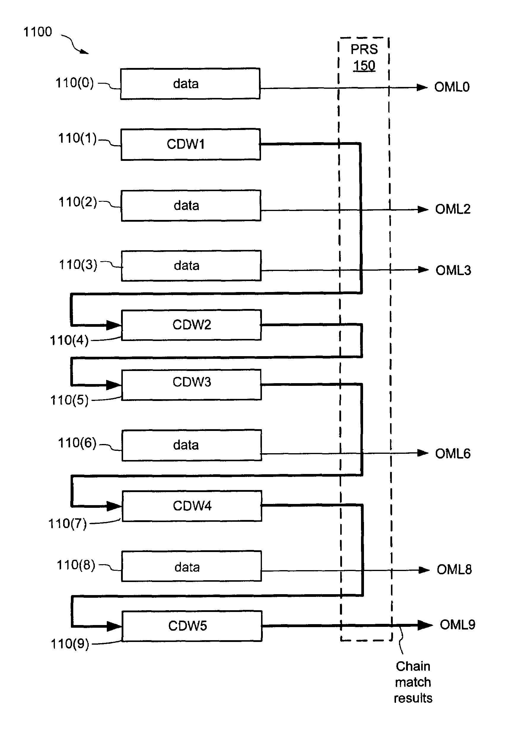
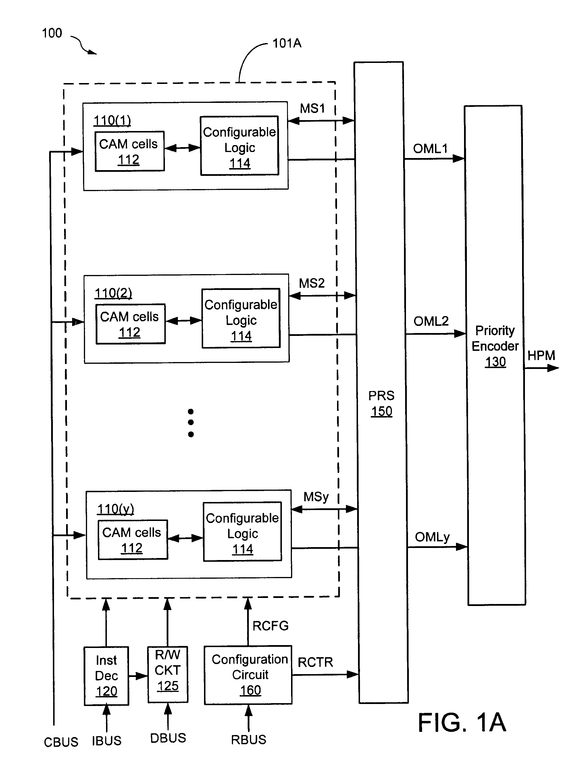
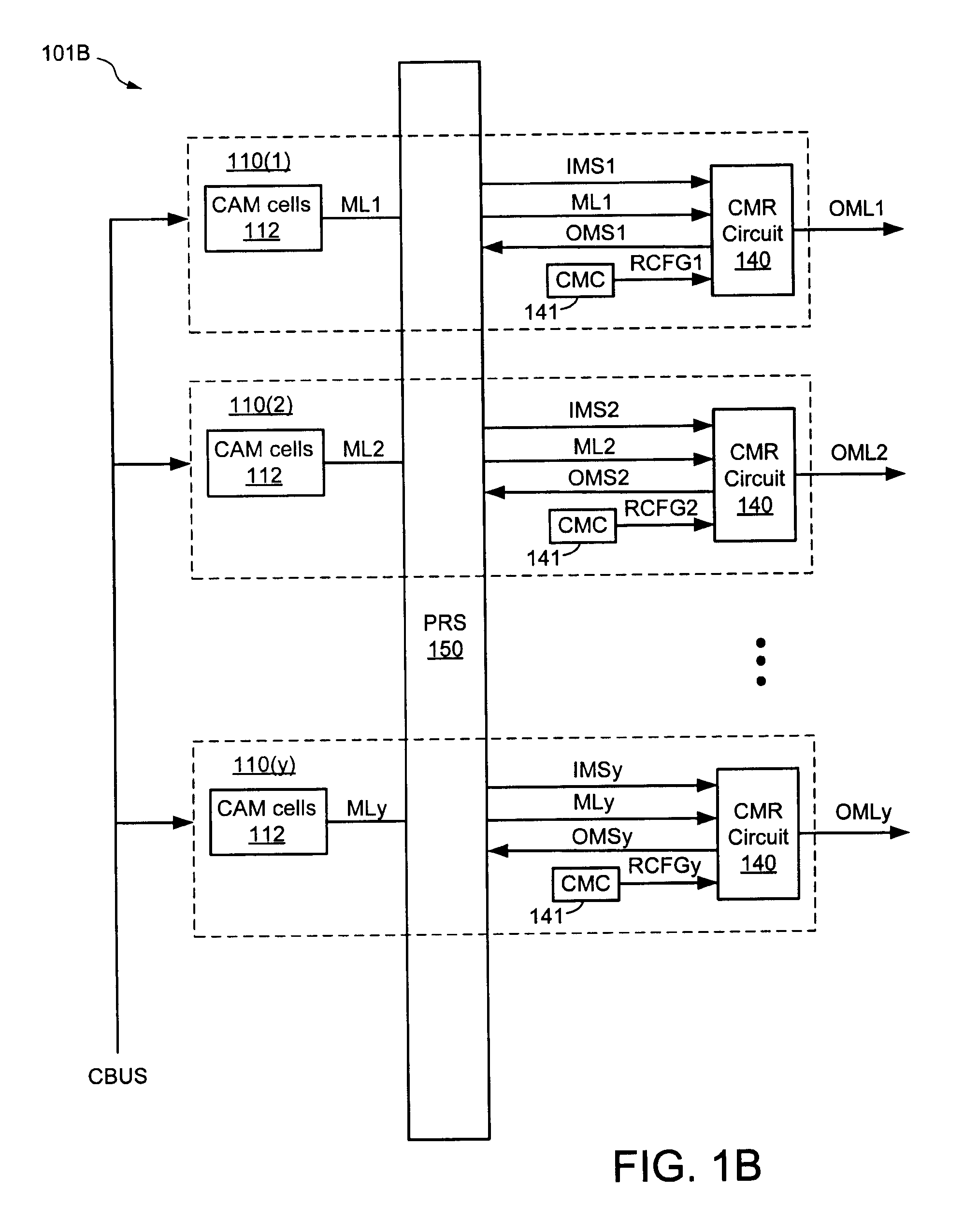
[0048]In the following description, numerous specific details are set forth such as examples of specific components, circuits, and processes to provide a thorough understanding of the present invention. In the following description, for purposes of explanation, specific nomenclature is set forth to provide a thorough understanding of the present invention. However, it will be apparent to one skilled in the art that these specific details may not be required to practice the present invention. In other instances, well-known circuits and devices are shown in block diagram form to avoid obscuring the present invention unnecessarily. It should be noted that the steps and operations discussed herein (e.g., the loading of registers) can be performed either synchronously or asynchronously. The term “coupled” as used herein means connected directly to or connected through one or more intervening components or circuits. Any of the signals provided over various buses described herein may be ti...


PUM


Abstract

A content addressable memory (CAM) device includes a plurality of CAM rows, a number of sequencing logic circuits, and a programmable interconnect structure. Each CAM row includes a number of CAM cells to generate a match signal on a match line and includes an enable input. Each sequencing logic circuit includes an input and an output, and is configured to count sequences of match signals from the CAM rows. The programmable interconnect structure selectively connects the match line of any CAM row to the input of any sequencing logic circuit, and selectively connects the output of any sequencing logic circuit to the enable input of any CAM row.

Description

CROSS-REFERENCE TO RELATED APPLICATIONS[0001]This application is a divisional of, and clams the benefit under 35 USC 120, of the co-pending and commonly owned U.S. patent application Ser. No. 12 / 131,992 entitled “Content Addressable Memory Device Having Programmable Interconnect Structure” filed on Jun. 3, 2008, which is incorporated by reference herein.FIELD OF INVENTION[0002]The present invention relates generally to content addressable memory (CAM) devices, and more particularly to CAM devices having an inter-row configurability feature that allows for the interconnection of any number of arbitrarily selected rows without regard to the physical locations of the rows relative to one another.BACKGROUND OF RELATED ART[0003]A content addressable memory (CAM) system is a storage system that can be instructed to compare a specific pattern of comparand data with data stored in its associative CAM array. The entire CAM array, or segments thereof, is searched in parallel for a match with ...

Claims


Application Information

Patent Timeline
Patent Type & Authority Patents(United States)
IPC IPC(8): G11C15/00
CPCG11C15/00G11C15/04G11C15/046
Inventor JOSHI, SACHINBIRMAN, MARKSRINIVASAN, MAHESHWARANKHANNA, SANDEEPSRINIVASAN, VARADARAJAN
Owner AVAGO TECH WIRELESS IP SINGAPORE PTE
Why Eureka
Try Eureka