Non-volatile memory and method with memory planes alignment

Inactive Publication Date: 2005-06-30
SANDISK TECH LLC
View PDF47 Cites 244 Cited by
  • Summary
  • Abstract
  • Description
  • Claims
  • Application Information

AI Technical Summary

Benefits of technology

[0030] According to another aspect of the invention, in a nonvolatile memory with block management system that supports update blocks with non-sequential logical units, an index of the logical units in a non-sequential update block is buffered in RAM and stored periodically into the non-volatile memory. In one embodiment, the index is stored in a block dedicated for storing indices. In another embodiment, the index is stored in the update block itself. In yet another embodiment, the index is stored in the header of each logical unit. In another aspect, the logical units written after the last index update but before the next have their indexing information stored in the header of each logical unit. In this way, after a power outage, the location of recently written logical units can be determined without having to perform a scanning during initialization. In yet another aspect, a block is managed as partially sequential and partially non-sequential, directed to more than one logical subgroup.
[0031] According to another aspect of the invention,

Problems solved by technology

Thus, when a logical group is being updated, the distribution of logical units (an

Method used


Image

  • Non-volatile memory and method with memory planes alignment
  • Non-volatile memory and method with memory planes alignment
  • Non-volatile memory and method with memory planes alignment

Examples


Embodiment Construction

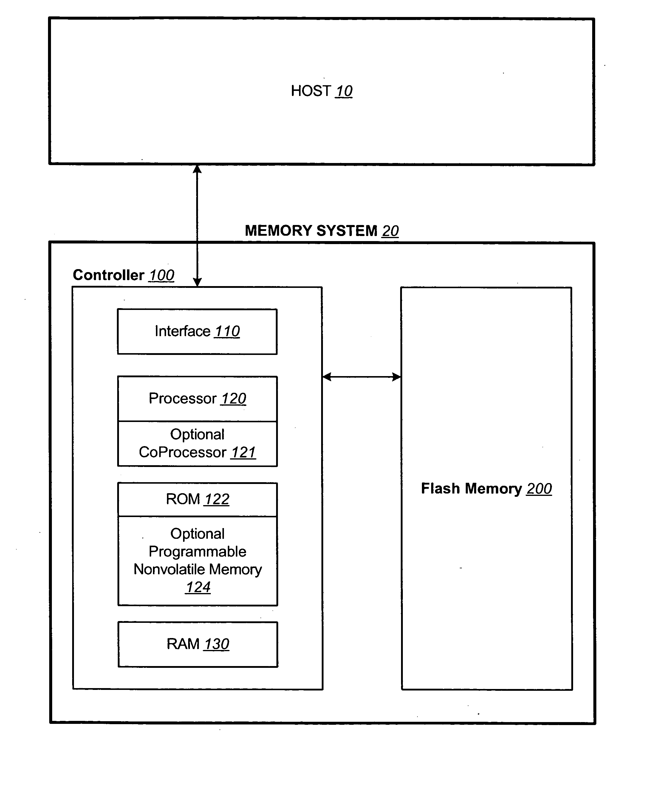
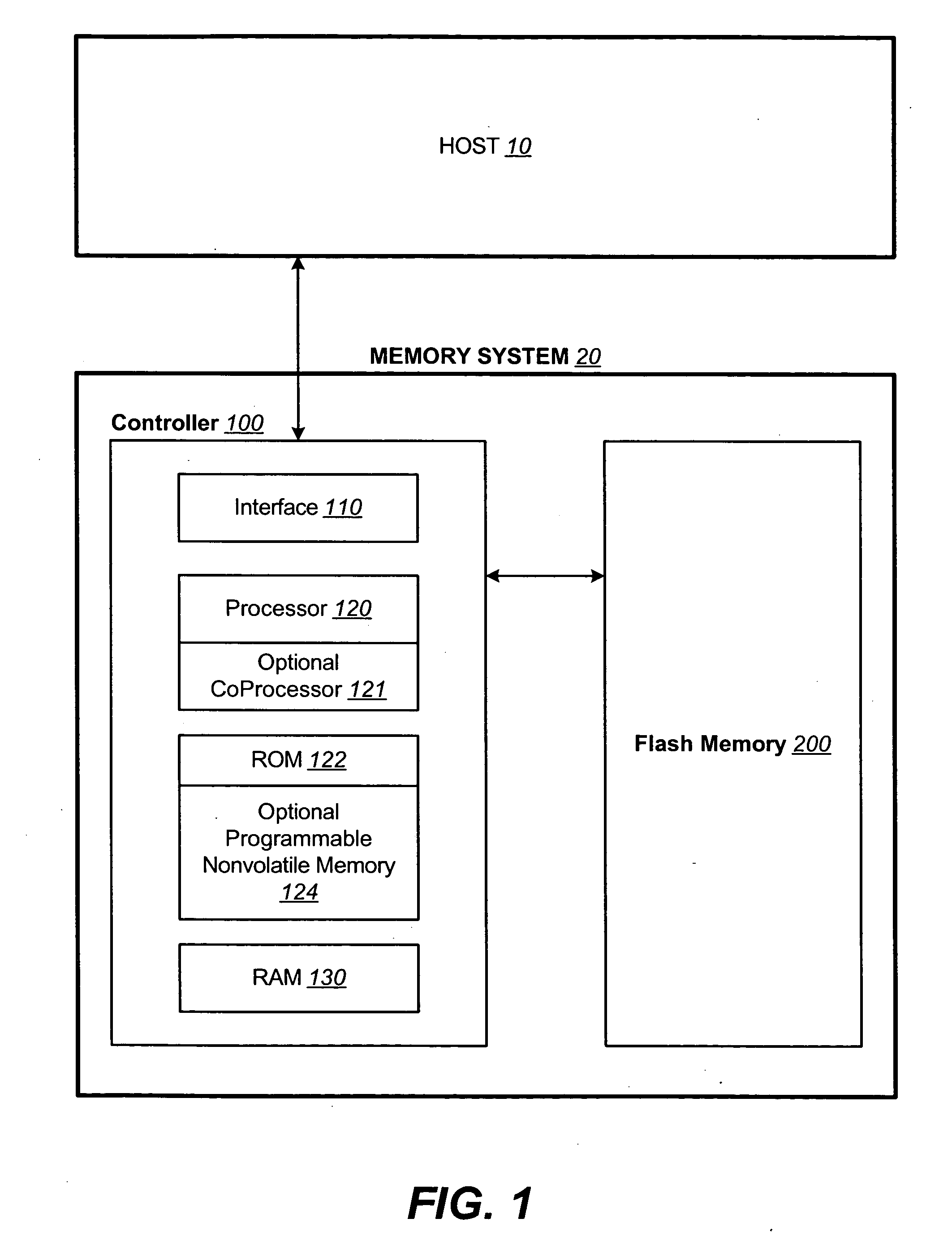
[0117]FIG. 1 illustrates schematically the main hardware components of a memory system suitable for implementing the present invention. The memory system 20 typically operates with a host 10 through a host interface. The memory system is typically in the form of a memory card or an embedded memory system. The memory system 20 includes a memory 200 whose operations are controlled by a controller 100. The memory 200 comprises of one or more array of non-volatile memory cells distributed over one or more integrated circuit chip. The controller 100 includes an interface 110, a processor 120, an optional coprocessor 121, ROM 122 (read-only-memory), RAM 130 (random access memory) and optionally programmable nonvolatile memory 124. The interface 110 has one component interfacing the controller to a host and another component interfacing to the memory 200. Firmware stored in nonvolatile ROM 122 and / or the optional nonvolatile memory 124 provides codes for the processor 120 to implement the ...


PUM


Abstract

A non-volatile memory is constituted from a set of memory planes, each having its own set of read/write circuits so that the memory planes can operate in parallel. The memory is further organized into erasable blocks, each for storing a logical group of logical units of data. In updating a logical unit, all versions of a logical unit are maintained in the same plane as the original. Preferably, all versions of a logical unit are aligned within a plane so that they are all serviced by the same set of sensing circuits. In a subsequent garbage collection operation, the latest version of the logical unit need not be retrieved from a different plane or a different set of sensing circuits, otherwise resulting in reduced performance. In one embodiment, any gaps left after alignment are padded by copying latest versions of logical units in sequential order thereto.

Description

CROSS REFERENCE TO RELATED APPLICATIONS [0001] This application is a continuation-in-part of U.S. patent application Ser. No. 10 / 750,155, filed on Dec. 30, 2003.FIELD OF THE INVENTION [0002] This invention relates generally to non-volatile semiconductor memory and specifically to those having a memory block management system optimized for operating multiple memory planes in parallel, where each plane is serviced by its own set of read / write circuits. BACKGROUND OF THE INVENTION [0003] Solid-state memory capable of nonvolatile storage of charge, particularly in the form of EEPROM and flash EEPROM packaged as a small form factor card, has recently become the storage of choice in a variety of mobile and handheld devices, notably information appliances and consumer electronics products. Unlike RAM (random access memory) that is also solid-state memory, flash memory is non-volatile, and retaining its stored data even after power is turned off. Also, unlike ROM (read only memory), flash m...

Claims


Application Information

Patent Timeline
IPC IPC(8): G06F11/20G06F12/02G11C7/00G11C11/56G11C16/10G11C16/34G11C29/00
CPCG06F11/1072G11C2211/5641G06F11/1415G06F11/1658G06F11/1666G06F12/0246G06F2212/7202G06F2212/7203G06F2212/7205G06F2212/7208G11C11/5621G11C11/5628G11C16/102G11C16/105G11C16/20G11C29/00G11C29/76G06F11/141G11C16/16G11C16/10
Inventor GOROBETS, SERGEY ANATOLIEVICHSMITH, PETER JOHNBENNETT, ALAN DAVID
Owner SANDISK TECH LLC
Why Eureka
Try Eureka