Air gap under on-chip passive device

a passive device and air gap technology, applied in the field of microelectronics, can solve the problems of weakening or breaking of metal lines, affecting the air gap process, and affecting the arrangement shown in the article by chen

Inactive Publication Date: 2010-02-16
GLOBALFOUNDRIES US INC
View PDF9 Cites 31 Cited by
  • Summary
  • Abstract
  • Description
  • Claims
  • Application Information

AI Technical Summary

Problems solved by technology

One problem of the structure shown in FIGS. 1A and 1B is the close proximity to the inductor 10 of dielectric materials in ILD layers which do not have low dielectric constants.
Prior attempts to address this problem have led to other problems.
The arrangement shown in the article by Chen is subject to various problems.
Mechanical stresses such as shock and vibration, as well as thermal expansion and contraction stresses, can cause the metal lines to move relative to each other and potentially cause the metal lines to weaken or break.
In addition, the process of making the air gap is not robust.
This may cause the finished inductor to exhibit inconsistent performance.

Method used


Image

  • Air gap under on-chip passive device
  • Air gap under on-chip passive device
  • Air gap under on-chip passive device

Examples


Embodiment Construction

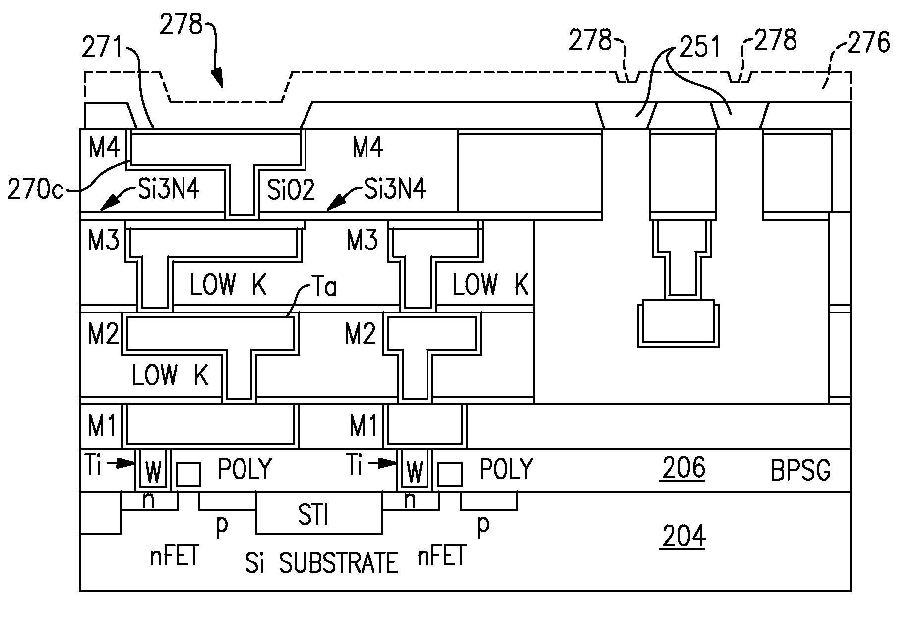
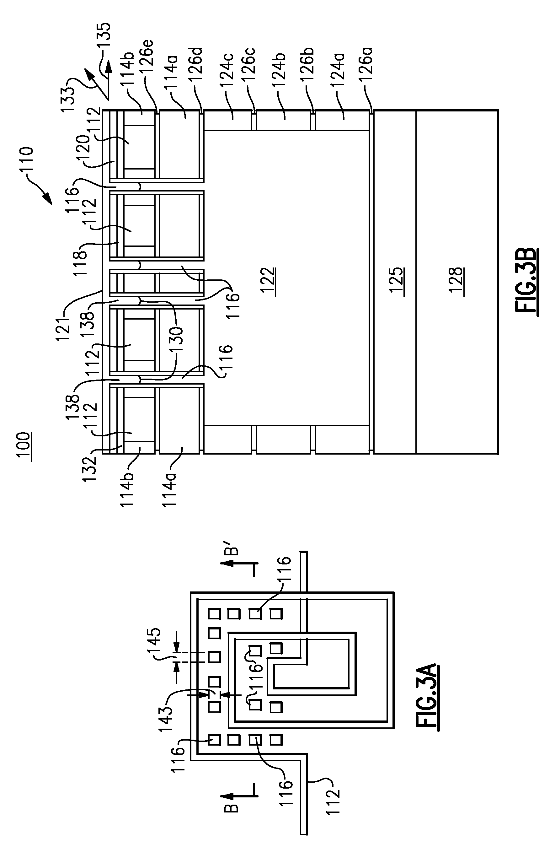
[0030]A microelectronic chip 100 in accordance with an embodiment of the invention is illustrated in FIGS. 3A and 3B. The chip includes a semiconductor region 128 in which active devices are provided, which may be conductively connected together in form of an integrated circuit. A passive device 110, e.g., an inductor, includes a plurality of metal patterns 112 which overlie the semiconductor region 128. As illustrated in FIG. 3B, the metal patterns 112 preferably include or consist essentially of a metal such as copper and are disposed in an “inorganic” interlevel dielectric (“ILD”) layer 114b, the ILD layer 114b illustratively including an inorganic dielectric material such as silicon dioxide, SiCOH, porous SiCOH, fluorinated silicon dioxide (“FSG”), porous silicon dioxide, and the like. Another inorganic ILD layer 114a is disposed underneath and adjacent to the ILD layer 114b. At least one, and preferably, a plurality of low-K ILD layers, e.g., ILD layers 124a, 124b, 124c, etc., ...


PUM


Abstract

A method is provided for fabricating a microelectronic chip which includes a passive device such, as an inductor, overlying an air gap. In such method, a plurality of front-end-of-line (“FEOL”) devices are formed in a semiconductor region of the microelectronic chip, and a plurality of stacked interlevel dielectric (“ILD”) layers are formed to overlie the plurality of FEOL devices, the plurality of stacked ILD layers including a first ILD layer and a second ILD layer, where the second ILD layer is resistant to attack by a first etchant which attacks the first ILD layer. A passive device is formed to overlie at least the first ILD layer. Using the first etchant, a portion of the first ILD layer in registration with the passive device is removed to form an air gap which underlies the passive device in registration with the passive device.

Description

BACKGROUND OF THE INVENTION[0001]The present invention relates to microelectronics, and more specifically to a structure and method for providing an air gap for enhancing performance of an on-chip passive device overlying a semiconductor region of a semiconductor integrated circuit chip.[0002]Techniques exist for providing passive devices, e.g., inductors, capacitors and / or resistors in a layer or region of an integrated circuit chip which overlies a semiconductor region in which active devices are provided. However, the performance of inductors and capacitors on such chips can be constrained by the type of dielectric material that is used to isolate their conductive portions from other features of the chip. For example, in the prior art chip illustrated in FIGS. 1A-1B, an inductor 10 includes a metal feature or other conductive feature which extends in a spiral pattern within a region 12 of a solid dielectric material which overlies a semiconductor region 14 of a microelectronic su...

Claims


Application Information

Patent Timeline
Patent Type & Authority Patents(United States)
IPC IPC(8): H01L21/302
CPCH01L21/7682H01L23/5222H01L23/5227H01L23/53295H01L27/0688H01L28/10H01L2924/0002H01L2924/00
Inventor STAMPER, ANTHONY K.CHINTHAKINDI, ANIL K.COOLBAUGH, DOUGLAS D.DALTON, TIMOTHY J.EDELSTEIN, DANIEL C.ESHUN, EBENEZER E.GAMBINO, JEFFREY P.MURPHY, WILLIAM J.VAED, KUNAL
Owner GLOBALFOUNDRIES US INC
Why Eureka
Try Eureka