Spin transistor using ferromagnet

a ferromagnetic and spin transistor technology, applied in the field of spin transistors, can solve the problems of substantial noise of spin transistors, low injection efficiency, and physical limit of oxide films, and achieve the effects of reducing contact resistance, clear spin transport signals, and reducing the thickness of the energy barrier between the source and the channel

Inactive Publication Date: 2010-03-09
KOREA INST OF SCI & TECH
View PDF8 Cites 4 Cited by
  • Summary
  • Abstract
  • Description
  • Claims
  • Application Information

AI Technical Summary

Benefits of technology

[0021]As apparent from the above description, according to the present invention, the ferromagnetic source and drain extend downwardly to or under a first upper cladding layer, making it easier for electrons injected from the ferromagnetic source to surmount an energy barrier. In other words, an energy barrier between the source and the channel is reduced in thickness. With this structure, the spin transistor has significantly reduced contact resistance, noticeably clear spin transport signal, and an improved signal-to-noise ratio. As a result, the spin transistor of the invention provides clear spin signals and a wide reading margin.

Problems solved by technology

Currently, MOSFET, one of the most important elements of a semiconductor device, is confronted with problems including difficulty in additional reduction of power and area, and a physical limit of an oxide film thereof.
According to this investigation, the spin transistor has problems of substantial noise and very low injection efficiency.
The high noise and very low injection efficiency is mainly caused by mismatch of conductivity between the metallic ferromagnet and the semiconductor, and by noise from a non-uniform junction therebetween.
Accordingly, the transistor suffers from deterioration in signal sensitivity, increase in power consumption, and reduction in signal-to-noise ratio.
As a result, it is difficult to stably obtain clear signals from the spin transistor 50.

Method used


Image

  • Spin transistor using ferromagnet
  • Spin transistor using ferromagnet
  • Spin transistor using ferromagnet

Examples


Embodiment Construction

[0040]Preferred embodiments will now be described in detail with reference to the accompanying drawings. It should be noted that the embodiments of the invention can take various forms, and that the present invention is not limited to the embodiments described herein. The embodiments of the invention are described so as to enable those having an ordinary knowledge in the art to have a perfect understanding of the invention. Accordingly, shape and size of components of the invention are enlarged in the drawings for clear description of the invention. Like components are denoted by the same reference numerals throughout the drawings.

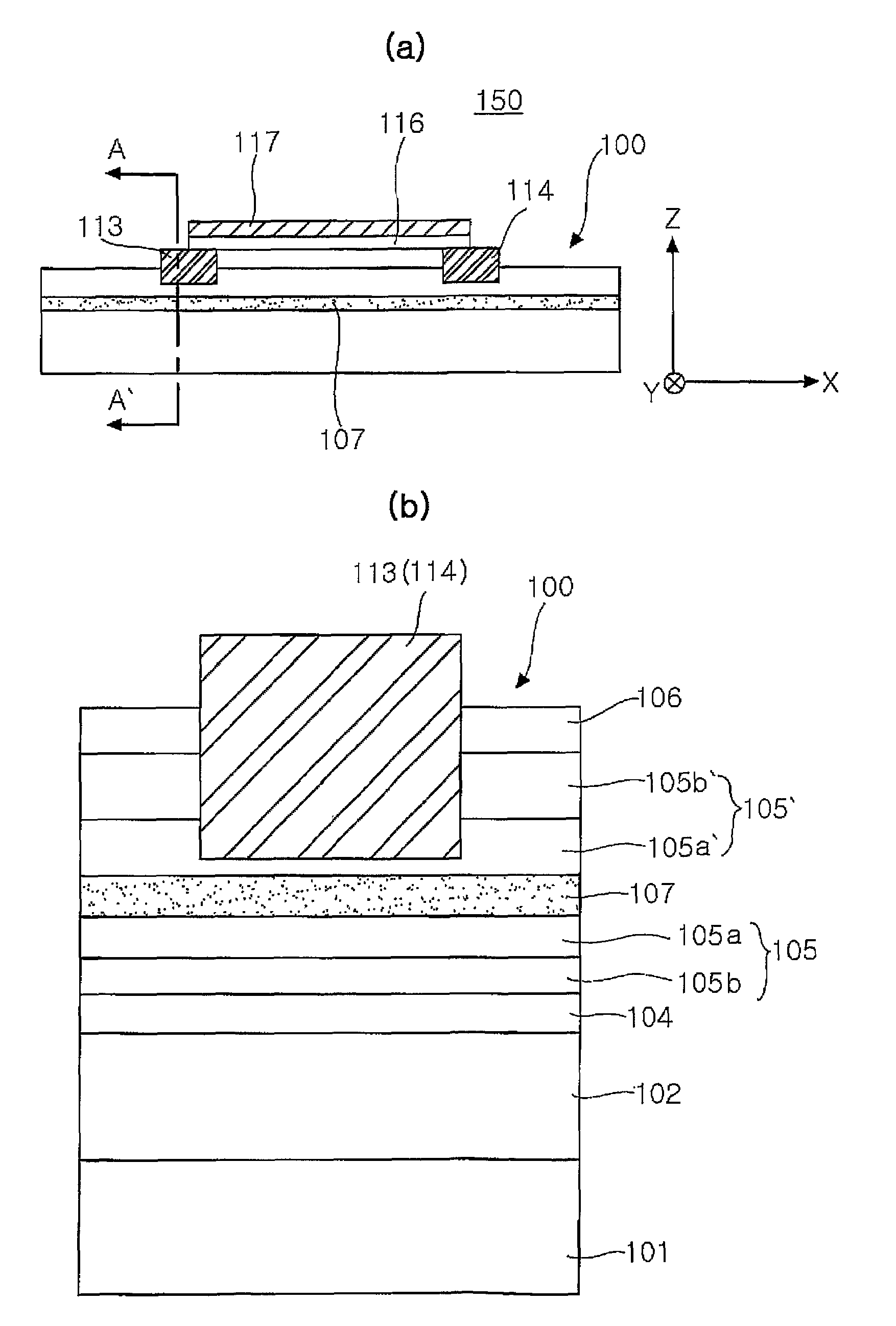
[0041]FIG. 4(a) is a cross-sectional view of a spin transistor according to one embodiment of the present invention, and FIG. 4(b) is a cross-sectional view taken along line AA′ of FIG. 4(a).

[0042]Referring to FIG. 4(a), a spin transistor 150 comprises a semiconductor substrate part 100 having a channel layer 107 formed therein, and a ferromagnetic source ...


PUM


Abstract

A spin transistor comprises a semiconductor substrate part having a lower cladding layer, a channel layer and an upper cladding layer sequentially stacked therein, a ferromagnetic source and drain on the substrate part, and a gate on the substrate part to control spins of electrons passing through the channel layer. The lower cladding layer comprises a first lower cladding layer and a second lower cladding layer having a higher band gap than that of the first lower cladding layer. The upper cladding layer comprises a first upper cladding layer and a second upper cladding layer having a higher band gap than that of the first upper cladding layer. The source and the drain are buried in an upper surface of the substrate part and extend downwardly to or under the first upper cladding layer.

Description

RELATED PATENT DATA[0001]This application claims priority to Patent Cooperation Treaty application Serial No. PCT / KR2006 / 004462, which was filed Oct. 30, 2006, and which claims priority to Korean Application Serial No. 10-2006-0057043, which was filed Jun. 23, 2006.TECHNICAL FIELD[0002]The present invention generally relates to a spin transistor comprising a ferromagnetic source and drain, and, more particularly, to a spin transistor, which shows clear spin transport from a ferromagnet to a semiconductor and an improved signal-to-noise ratio.BACKGROUND ART[0003]Recently, a spin transistor such as Spin-FET (field effect transistor) has been spotlighted under active investigation as a new concept transistor. A conventional semiconductor-based transistor (for example, MOSFET) controls charges in the semiconductor by use of an electric field, whereas the spin transistor simultaneously controls both charges and spins by use of spin-polarized charges. Today's investigations try to apply t...

Claims


Application Information

Patent Timeline
Patent Type & Authority Patents(United States)
IPC IPC(8): H01L29/00
CPCH01L29/66984H01L29/7787H01L27/105H01L29/82
Inventor KOO, HYUN-CHEOLHAN, SUK-HEEEOM, JONG-HWACHANG, JOON-YEONKIM, HYUNG-JUNYI, HYUN-JUNG
Owner KOREA INST OF SCI & TECH
Why Eureka
Try Eureka