
Luminous device including conductive film

a conductive film and luminous device technology, applied in the direction of discharge tube/lamp details, discharge tube luminescnet screens, other domestic articles, etc., can solve the problems of inability to easily generate noise, unnecessary backlight, and inability to drive luminous elements by dc voltage, so as to improve the capability of injecting electrons

Inactive Publication Date: 2006-11-07
SEMICON ENERGY LAB CO LTD
View PDF21 Cites 4 Cited by
  • Summary
  • Abstract
  • Description
  • Claims
  • Application Information

AI Technical Summary

Benefits of technology

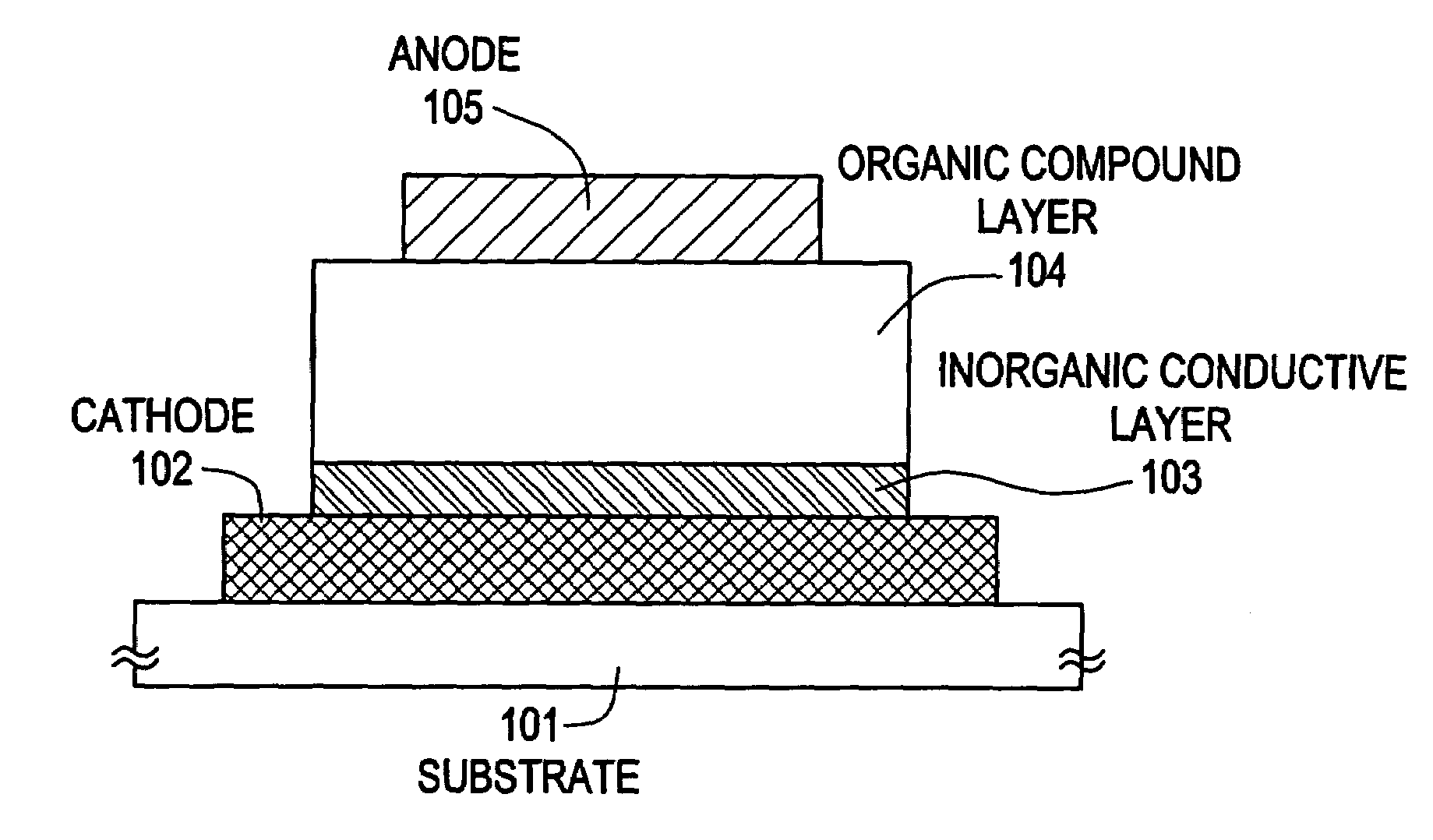
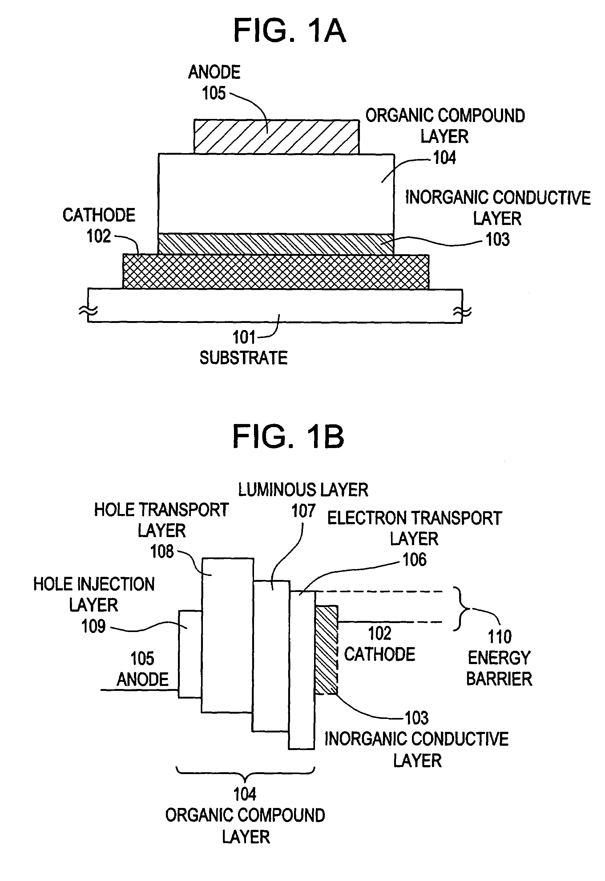
The present invention solves problems in the production of luminous elements by forming a new layer instead of a conventional cathode buffer layer. An inorganic conductive layer made of a substance with a smaller work function than the cathode and an electric conductivity of 1×10⁻¹⁰ S / m or more is used instead of a cathode buffer layer. This improves the capability of injecting electrons from the cathode and solves problems of diffusion and low electric conductivity. The inorganic conductive layer is made of a material with a smaller work function and an electric conductivity of 1×10⁻¹⁰ S / m or more. The film thickness of the conductive film can be controlled, and a reduction in production costs and an improvement in yield can be achieved. The inorganic conductive layer can be formed between the organic compound layer and the cathode or between the organic compound layer and the anode. The organic compound layer can have a smaller electron affinity than metals, and an electrode with a small work function can be used to improve the capability of injecting electrons. The inorganic conductive film can have a smaller work function than the cathode, and both the cathode and the conductive film can have a thickness of 20 nm or less.

Problems solved by technology

Therefore, backlight, which is used in conventional liquid crystal displays, is unnecessary.
Since a luminous element is of a carrier injection type, the luminous element can be driven by DC voltage and noises are not easily generated.
All of the material systems are easily oxidized by water content in the atmosphere, so that a dark spot, which is a luminescence defect of the element, is generated or a rise in voltage occurs.
However, in the case in which any metal selected from alkali metals and alkali earth metals belonging to group I or group II in the periodic table is used alone for the cathode buffer layer, there arises a problem that the metal diffuses to have a bad effect on properties of a TFT connected to the luminous element.
Therefore, a scattering in the film thickness is easily generated in respective pixels, and it is difficult to control the film thickness.

Method used


Image

  • Luminous device including conductive film
  • Luminous device including conductive film
  • Luminous device including conductive film

Examples


embodiment 1

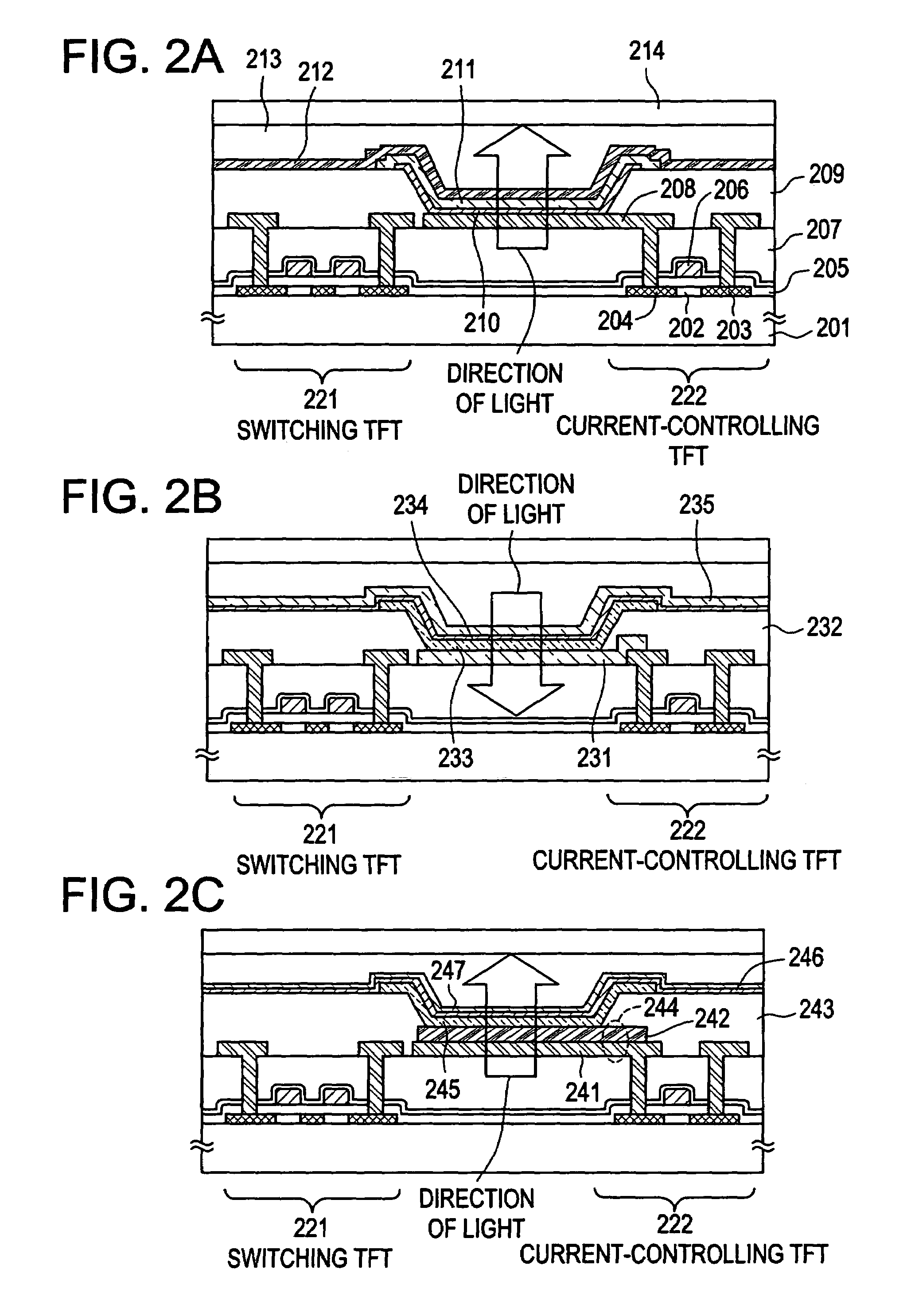
[0066]A sectional structure of a pixel section of a luminous device will be described as Embodiment 1 of the present invention, referring to FIG. 2A.

[0067]In FIG. 2A, semiconductor elements are formed on a substrate 201. As the substrate 201, a glass substrate having transparency is used. However, a quartz substrate may be used. As the semiconductor elements, TFTs are used. An active layer in each of the TFTs has at least a channel formed region 202, a source region 203 and a drain region 204.

[0068]The active layer in each of the TFTs is covered with a gate insulating film 205, and a gate electrode 206 overlapping the channel formed region 202 across the gate insulating film 205 is formed. An interlayer insulating film 207 covering the gate electrode 206 is deposited, and an electrode connected electrically to the source region or the drain region of each of the TFTs is formed on the interlayer insulating film 207. An electrode reaching a drain region 204 of a current-controlling TF...

embodiment 2

[0077]The following will describe a sectional structure of a pixel section of a luminous device as Embodiment 2 of the present invention, referring to FIG. 2B. The structure formed until the interlayer insulating film 207 is formed is the same as in Embodiment 1 except that the current-controlling TFT is formed to be of a p-channel type. Thus, detailed description thereof is omitted.

[0078]On the interlayer insulating film 207 is formed an electrode connected electrically to the source region or the drain region of each of the TFTs. An electrode reaching a drain region 204 of a current-controlling TFT 222, which is a p-channel type TFT, is connected electrically to an anode 231 of the luminous element. An insulating layer 232 having an opening which covers the edge portion of the anode 231 and has a tapered edge is deposited.

[0079]An organic compound layer 233 is deposited on the anode 231. An inorganic conductive layer 234 is deposited thereon. A cathode 235 is set up on the inorgan...

embodiment 3

[0083]The following will describe a sectional structure of a pixel section of a luminous device as Embodiment 3 of the present invention, referring to FIG. 2C. The structure formed until the interlayer insulating film 207 is formed is the same as in Embodiment 1 except that the current-controlling TFT is formed to be of a p-channel type. Thus, detailed description thereof is omitted.

[0084]In the present Embodiment 3, a first electrode 241 is formed connected electrically to each TFT. A material for forming the first electrode 241 is preferably any one selected from conductive materials having light-shading property and a high reflectivity, for example, aluminum, titanium, or tungsten. It is preferred to use a monolayer made of any one selected from the above-mentioned conductive materials or a lamination wherein two or more selected from the conductive materials.

[0085]A second electrode 242 made of a material having a large work function is formed on the first electrode 241. It is d...


PUM

PropertyMeasurementUnit
work functionaaaaaaaaaa
thicknessaaaaaaaaaa
thicknessaaaaaaaaaa

Abstract

Provided is a means for improving the capability of injecting electrons from a cathode in a luminous element and solving problems about the production process thereof. In the present invention, a material having a smaller work function than a cathode material is used to form an inorganic conductive layer between the cathode and an organic compound layer. In this way, the capability of injecting electrons from the cathode can be improved. Furthermore, the film thereof can be thicker than that of a conventional cathode buffer layer formed by using an insulating material. Therefore, the film thickness can easily be controlled, and a decrease in production costs and an improvement in yield can be achieved.

Description

BACKGROUND OF THE INVENTION[0001]1. Field of the Invention[0002]The present invention relates to a luminous device using a luminous element which has a film containing an organic compound (hereinafter referred to as an “organic compound layer”) between a pair of electrodes and which can give fluorescence or luminescence by receiving an electric field. The luminous device referred to in the present specification is an image display device, a luminescent device or a light source. Additionally, the following are included in examples of the luminous device: a module wherein a connector, for example, a flexible printed circuit (FPC) or a tape automated bonding (TAB) tape, or a tape carrier package (TCP)) is set up onto a luminous element; a module wherein a printed wiring board is set to the tip of a TAB tape or a TCP; and a module wherein integrated circuits (IC) are directly mounted on a luminous element in a chip on glass (COG) manner.[0003]2. Related Art[0004]A luminous element is an...

Claims


Application Information

Patent Timeline
Patent Type & Authority Patents(United States)
IPC IPC(8): H05B33/00H01L33/00H05B33/20H10K99/00
CPCH01L51/5092H01L27/3244Y10S428/917H10K59/12H10K50/171H05B33/20
Inventor SEO, SATOSHIIMAI, KEITARO
Owner SEMICON ENERGY LAB CO LTD
Learn More