

Method of operating a semiconductor memory device having a recessed control gate electrode
a technology of semiconductor memory and gate electrode, which is applied in the direction of semiconductor devices, digital storage, instruments, etc., can solve the problems of increasing the speed the source and drain region of the 3-d semiconductor memory device may also occupy a relatively large area, and achieves the effect of high reliability and efficiency
- Summary
- Abstract
- Description
- Claims
- Application Information
AI Technical Summary
Benefits of technology
Problems solved by technology
Method used
Image

Examples
Embodiment Construction
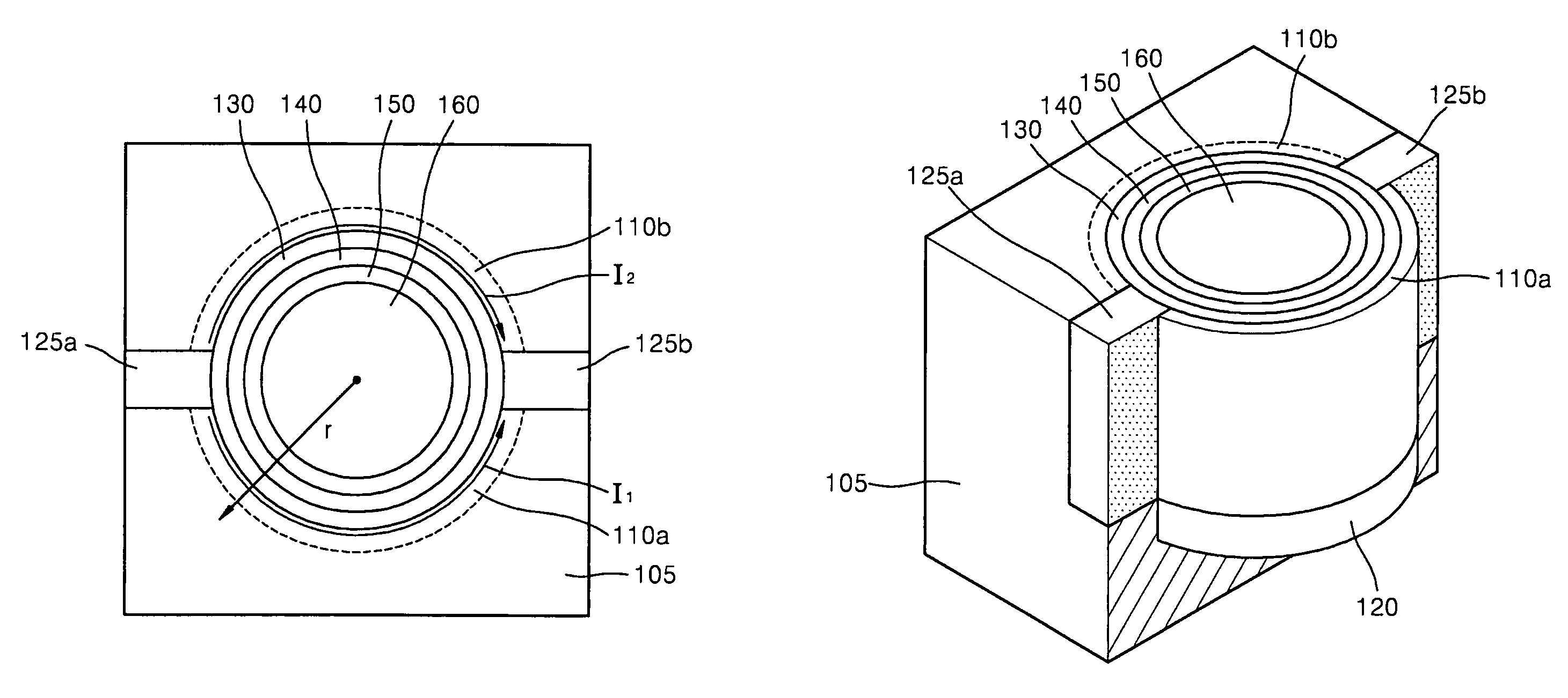
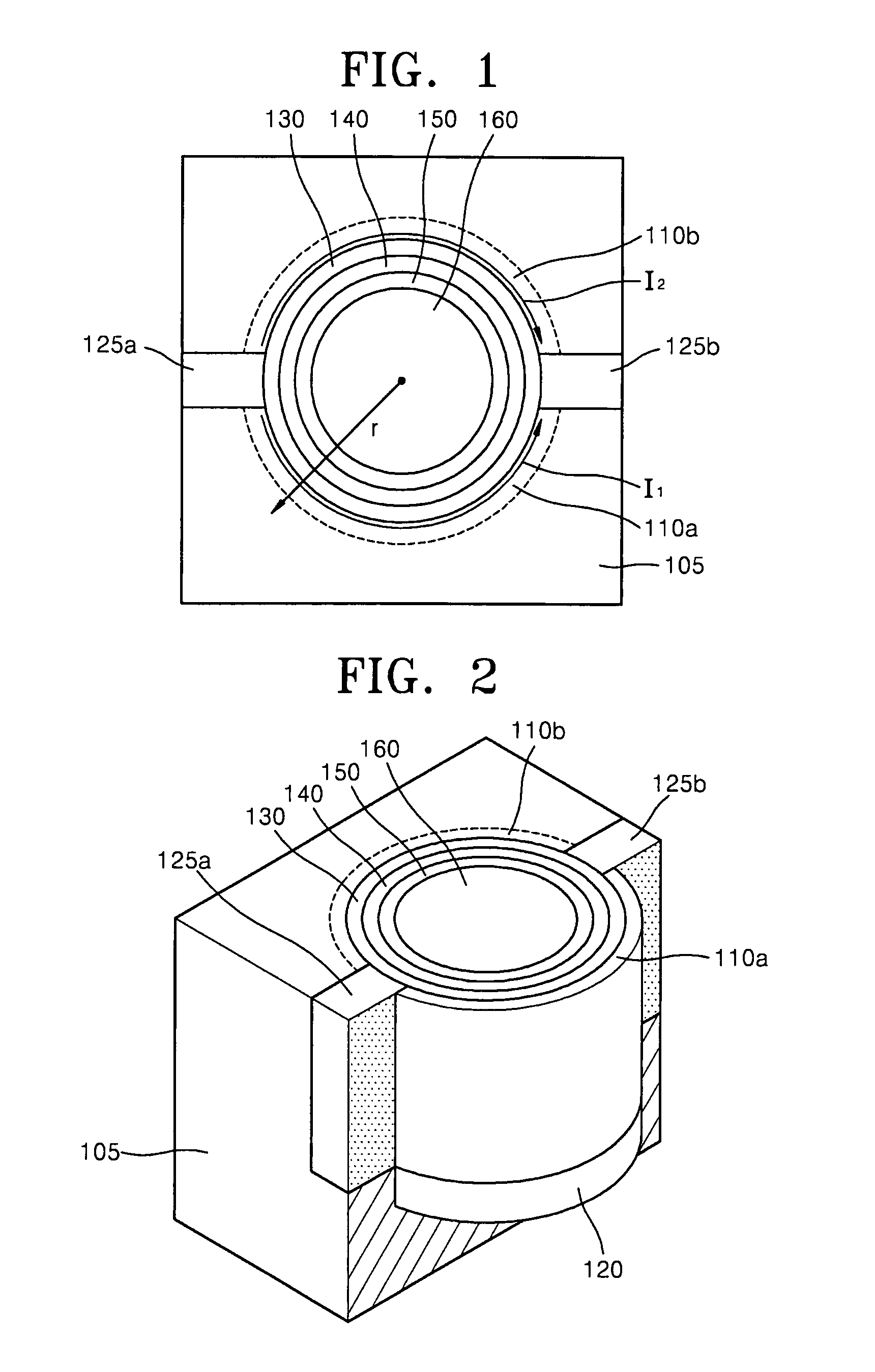
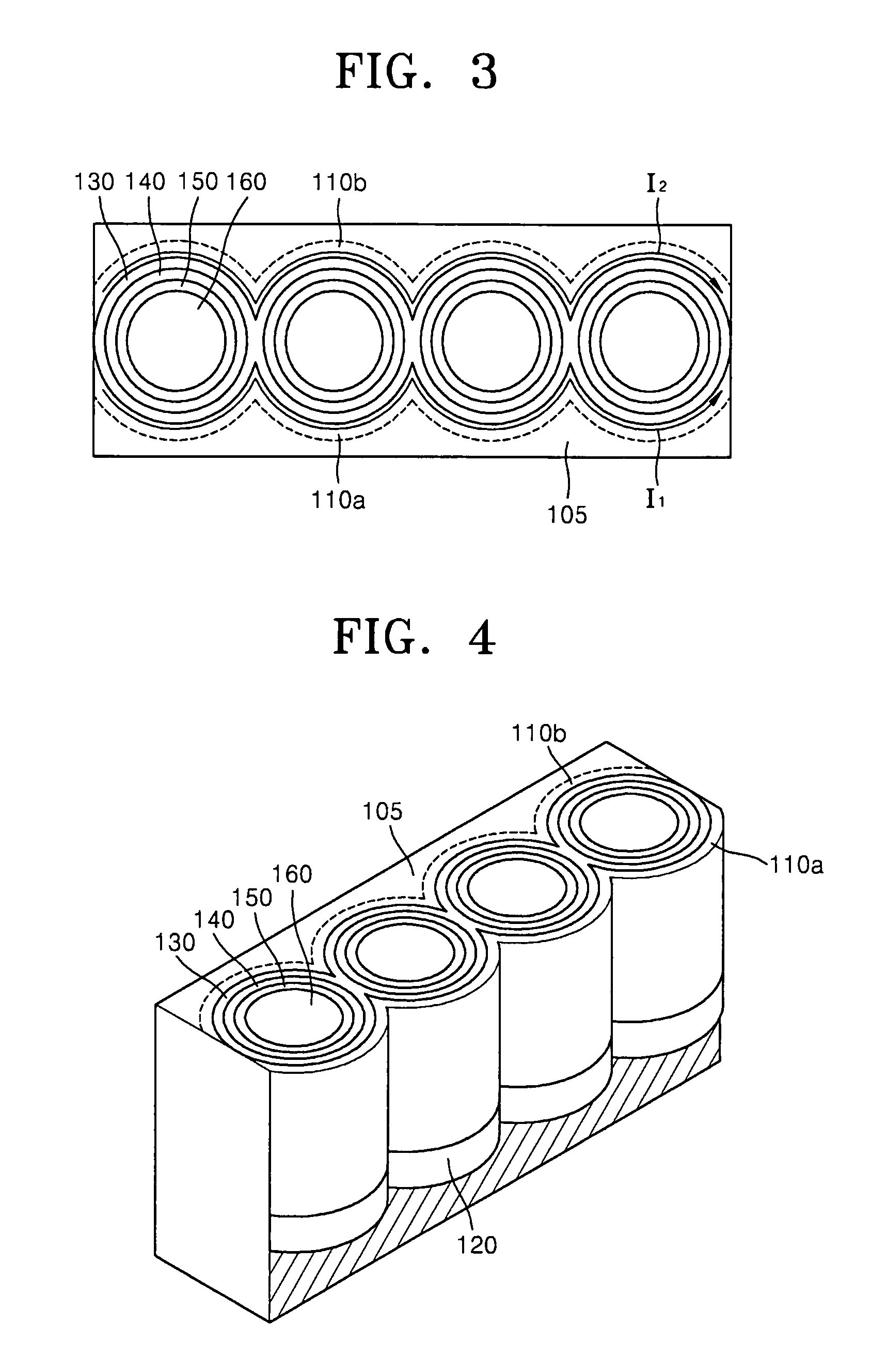
[0008]Example embodiments provide a method of operating a three-dimensional (3-D) semiconductor memory device having higher reliability and efficiency. A method of operating a semiconductor memory device may include providing a semiconductor memory device having a semiconductor substrate, a control gate electrode recessed in the semiconductor substrate, a storage node layer between the control gate electrode and the semiconductor substrate, a tunneling insulating layer between the storage node layer and the semiconductor substrate, a blocking insulating layer between the storage node layer and the control gate electrode, and / or first and second channel regions surrounding the control gate electrode and separated by a pair of opposing separating insulating layers; and programming data in the storage node layer by charge tunneling through the blocking insulating layer.
[0009]Programming the data may include applying a negative program voltage to the control gate electrode. Applying the...
PUM
 Abstract
Description
Claims
Application Information