

Voltage level shifter and buffer using same
buffer technology, applied in the direction of multiple-port active network, electric pulse generator, automatic control, etc., can solve the problems of limiting the frequency range for which a voltage level shifter is useful, and often losing efficiency to direct current (dc) power consumption
- Summary
- Abstract
- Description
- Claims
- Application Information
AI Technical Summary
Benefits of technology
Problems solved by technology
Method used
Image

Examples
Embodiment Construction
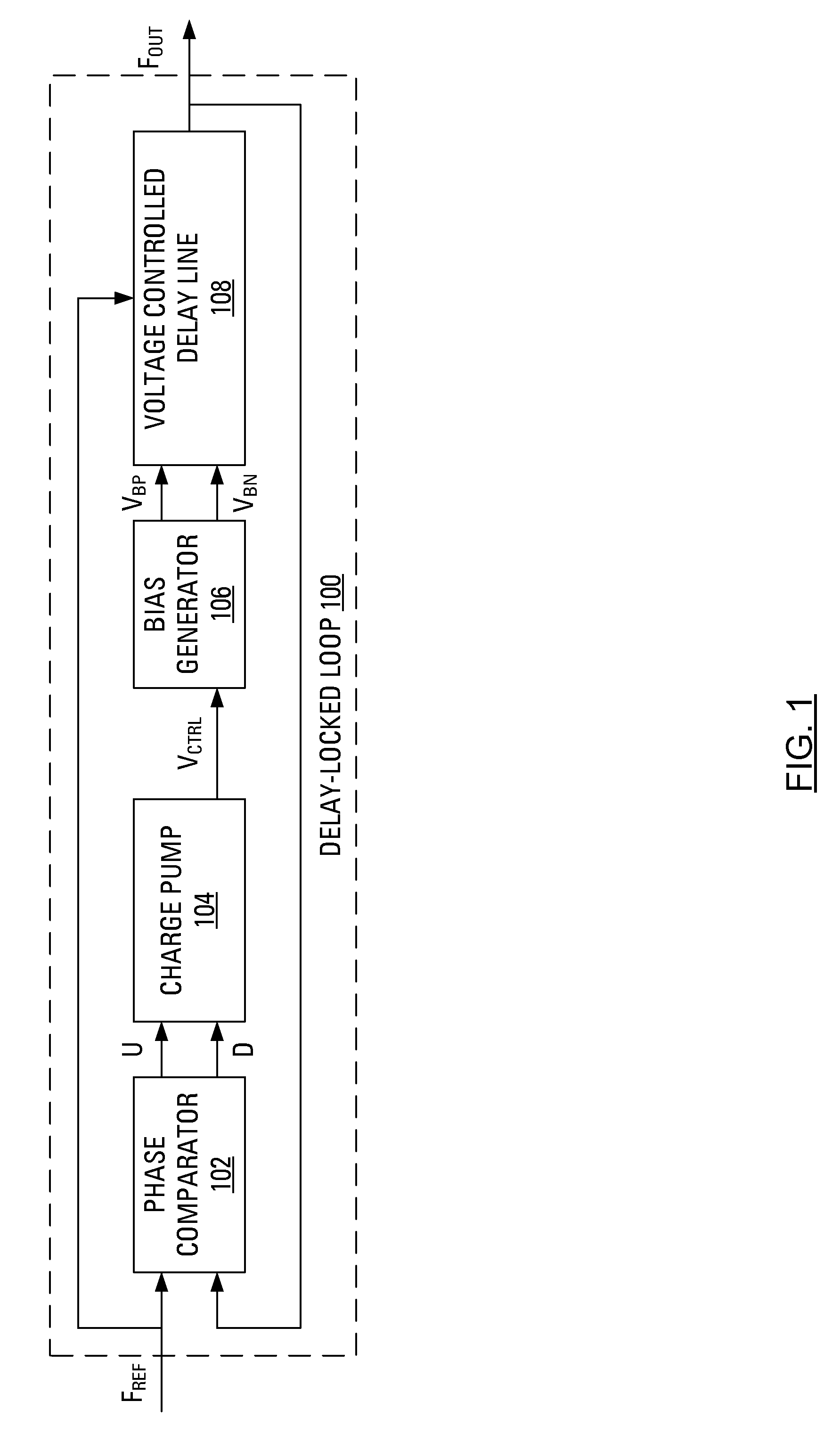
[0021]FIG. 1 presents a schematic illustration of a typical delay-locked loop (DLL) 100 as presented in John G. Maneatis, “Low-Jitter Process-Independent DLL and PLL Based on Self-Biased Technique”, IEEE JSSC VOL. 31, No 11, November 1996, pp. 1723-1732 (hereinafter “Maneatis”). Maneatis indicates that a self-biased DLL is constructed by taking advantage of the control relationship offered by a typical DLL. The typical DLL 100 includes a phase comparator 102, a charge pump 104, a loop filter, a bias generator 106 and voltage controlled delay line (VCDL) 108. The negative feedback in the loop adjusts the delay through the VCDL 108 by integrating the phase error that results between a periodic reference input, FREF, and output, FOUT, from the VCDL 108. Once in lock, the VCDL 108 will delay the reference input, FREF, by a fixed amount to form the VCDL output such that there is no detected phase error between FREF and FOUT.
[0022]In operation, the phase comparator 102 receives the AC ref...
PUM
 Abstract
Description
Claims
Application Information