Integrated circuit leadless package system

a leadless, integrated circuit technology, applied in printed circuits, semiconductor devices, semiconductor/solid-state device details, etc., can solve the problems of leadless packages being particularly susceptible to narrow lead-to-lead gaps, causing destructive pressure on ever shrinking dimensions, and plating being susceptible to shorting

Active Publication Date: 2010-03-23
STATS CHIPPAC LTD
View PDF16 Cites 31 Cited by
  • Summary
  • Abstract
  • Description
  • Claims
  • Application Information

AI Technical Summary

Problems solved by technology

Manufacturing the package includes many processes that create destructive pressure on ever shrinking dimensions.
This will cause the lead plating to be susceptible to shorting during the processing particularly when the package is clamped.
Small form factor packages or chip scale packages, such as bump chip carriers, land grid arrays, no-lead or leadless packages are particularly susceptible to narrow lead-to-lead gaps as well as reduced strength leads.
Higher numbers of leads and smaller sizes have made lead formation and encapsulation extremely difficult.
Many of the processing steps may deform the fragile leads resulting in missing, hard to reach or shorted connections.
The missing, hard to reach or shorted connections typically render the integrated circuit device useless.
This in turn will cause the solder plating to be more susceptible to shorting during a singulation process when the flange area is clamped.
The shorting caused by the plating of the top flange and the reduce lead-to-lead gap resulting in useless integrated circuit device, reduces performance, functions and manufacturing yields, thereby increasing costs, complexity and throughput.
Solutions to these problems have been long sought but prior developments have not taught or suggested any solutions and, thus, solutions to these problems have long eluded those skilled in the art.

Method used


Image

  • Integrated circuit leadless package system
  • Integrated circuit leadless package system
  • Integrated circuit leadless package system

Examples


Embodiment Construction

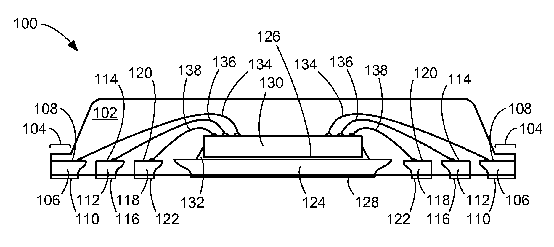
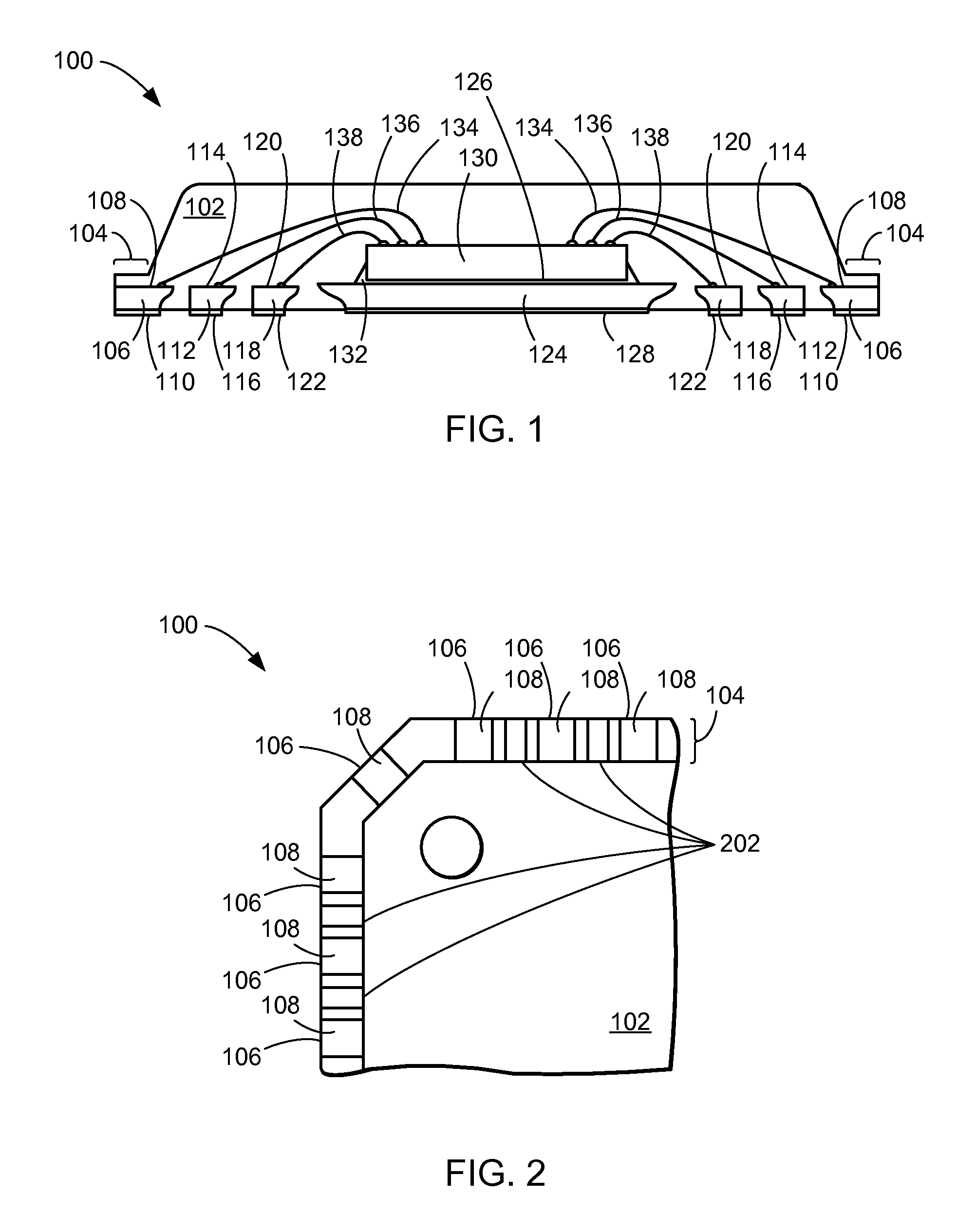
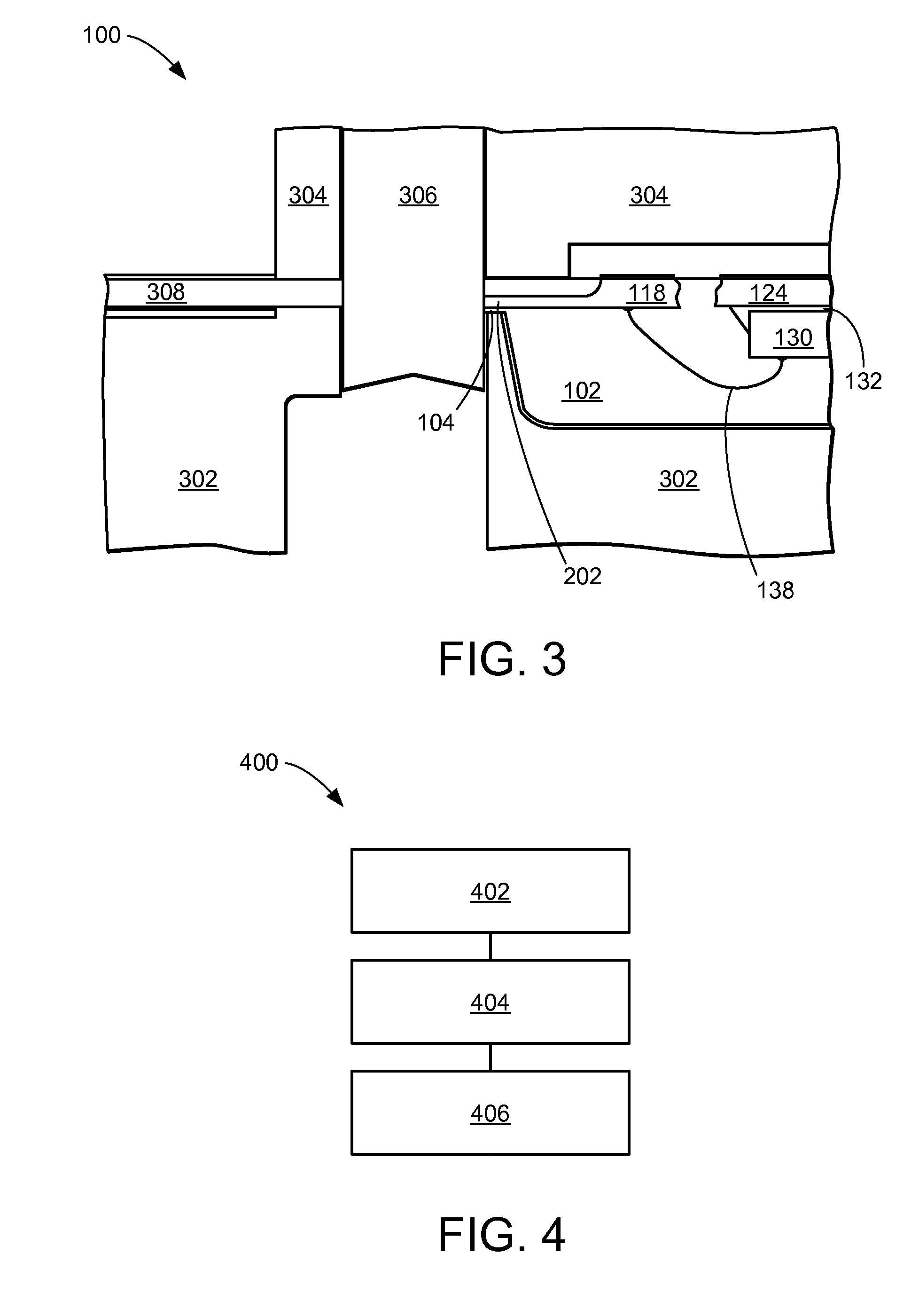
[0016]In the following description, numerous specific details are given to provide a thorough understanding of the invention. However, it will be apparent that the invention may be practiced without these specific details. In order to avoid obscuring the present invention, some well-known circuits, and process steps are not disclosed in detail.

[0017]Likewise, the drawings showing embodiments of the apparatus / device are semi-diagrammatic and not to scale and, particularly, some of the dimensions are for the clarity of presentation and are shown greatly exaggerated in the drawing FIGs. Similarly, although the sectional views in the drawings for ease of description show the invention with surfaces as oriented downward, this arrangement in the FIGs. is arbitrary and is not intended to suggest that invention should necessarily be in a downward direction. Generally, the device can be operated in any orientation. In addition, the same numbers are used in all the drawing FIGs. to relate to ...


PUM


Abstract

An integrated circuit leadless package system includes forming a lead, attaching an integrated circuit die to the lead, and applying an encapsulant including a thin encapsulant region with a thinner section over the lead than a section over the integrated circuit die.

Description

TECHNICAL FIELD[0001]The present invention relates generally to package systems, and more particularly to a system for an integrated circuit leadless package.BACKGROUND ART[0002]Consumer and industry demands for more functions, lower cost, and smaller form factors have increased use of integrated circuits. Integrated circuits today are used in very small systems, such as cell phones, music players, and cameras, to very large systems, such as cars, airplanes, and industrial controls. Across virtually all applications, there continues to be demand for reducing the size and increasing performance of the devices. The intense demand is no more visible than in portable electronics that have become so ubiquitous.[0003]Smaller integrated circuit devices require a smaller package, which both encases the circuit and provides electrical interconnection to external circuitry. A leadframe is one common means of electrical interconnection. The leadframe is formed from electrically conductive mate...

Claims


Application Information

Patent Timeline
Patent Type & Authority Patents(United States)
IPC IPC(8): H01L23/495H01L23/28
CPCH01L21/4842H01L23/3107H01L23/49548H01L2224/32245H01L2224/48091H01L2224/48247H01L2224/73265H01L2924/01078H01L2924/00014H01L24/48H01L2924/14H01L2924/181H01L2224/48465H01L2924/18301H01L2924/00H01L2924/00012H01L2224/45099H01L2224/45015H01L2924/207
Inventor LAU, KENG KIAT
Owner STATS CHIPPAC LTD
Why Eureka
Try Eureka