Communication board

a communication board and board technology, applied in the field of communication boards, can solve the problems of data latency increase, data transfer rate restriction, data limit to a frequency, etc., and achieve the effect of high speed and facilitate the transmission and/or reception of large-capacity information

Inactive Publication Date: 2010-05-11
SONY CORP
View PDF1 Cites 26 Cited by
  • Summary
  • Abstract
  • Description
  • Claims
  • Application Information

AI Technical Summary

Benefits of technology

[0013]Thus, an embodiment of the present invention facilitates transmitting and / or receiving large-capacity information between electronic devices with high speed.

Problems solved by technology

Electrical-wiring communications using a narrow bus are often performed between electronic devices due to an electrical trouble and / or a mechanical trouble which occurs in a signal-connection unit of an interface.
In that case, there is a limit to a frequency due to impedance mismatching which occurs in wiring and / or a junction and the data-transfer rate is restricted.
Subsequently, the data latency increases, which makes it difficult to transmit and / or receive large-capacity information with high speed.

Method used


Image

  • Communication board
  • Communication board
  • Communication board

Examples


Embodiment Construction

[0032]Before describing embodiments of the present invention, the correspondence between the features of the claims and the specific elements disclosed in embodiments of the present invention is discussed below. This description is intended to assure that specific elements disclosed in an embodiment supporting the claimed invention are described in this specification. Thus, even if an element in an embodiment is not described as relating to a certain feature of the present invention, that does not necessarily mean that the element does not relate to that feature of the claims. Conversely, even if an element is described herein as relating to a certain feature of the claims, that does not necessarily mean that the element does not relate to other features of the claims.

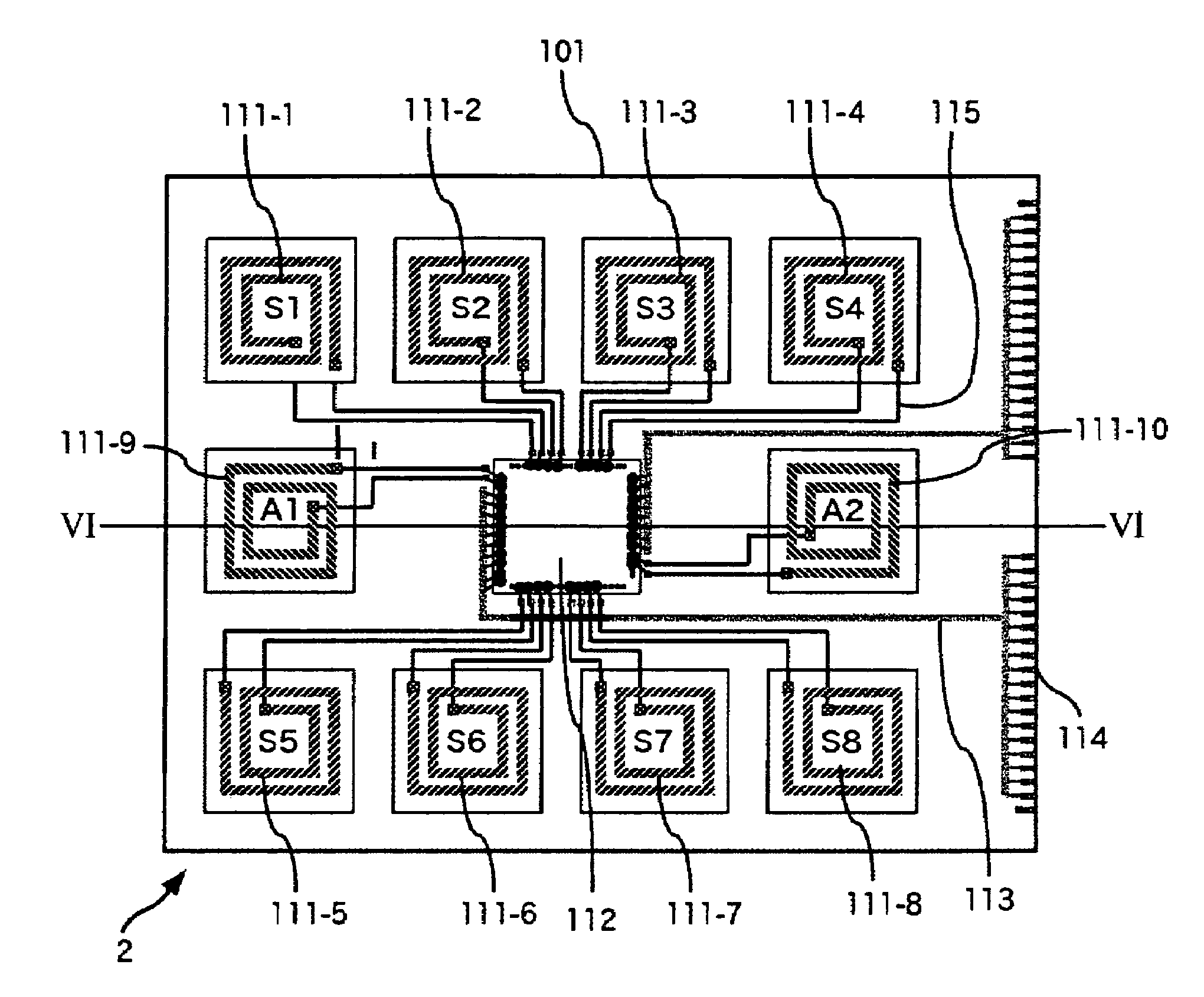
[0033]For example, a communication board 2-1 according to an embodiment of the present invention is configured, as shown in FIG. 1. Namely, the communication board 2-1 includes a plurality of antennas 111 shown in FIG....


PUM


Abstract

A communication board mounted on an electronic device includes a plurality of antennas configured to transmit and / or receive a signal by electromagnetic induction, where each of the plurality of antennas is provided on a substrate, as a coil-shaped pattern, a semiconductor chip mounted on the substrate, the semiconductor chip including at least one of a transmission circuit which transmits a signal to the antenna and a reception circuit which receives a signal transmitted from the antenna, and an input-and-output end that is connected to the semiconductor chip via a wiring layer provided on the substrate and an electronic circuit of the electronic device. The communication board communicates with a communication board mounted on another electronic device via the antenna by electromagnetic induction.

Description

CROSS REFERENCES TO RELATED APPLICATIONS[0001]The present invention contains subject matter related to Japanese Patent Application JP 2005-195444 filed in the Japanese Patent Office on Jul. 4, 2005, the entire contents of which are incorporated herein by reference.BACKGROUND OF THE INVENTION[0002]1. Field of the Invention[0003]The present invention relates to a communication board and particularly relates to a communication board that can perform high-speed communications, so as to easily transmit and / or receive large-capacity data between electronic devices.[0004]2. Description of the Related Art[0005]The applicant of the present invention had proposed technologies for adding and changing the function of an electronic device by mounting a removable block onto the electronic block, and changing the block and / or adding another block for mounting, as disclosed in Japanese Unexamined Patent Application Publication No. 2003-333541. The above-described technologies facilitate adding and / ...

Claims


Application Information

Patent Timeline
Patent Type & Authority Patents(United States)
IPC IPC(8): G06K7/08
CPCH01L23/49838H01L23/538H01L25/0652H01L25/0657H01L25/105H01L25/16H01Q1/2258H01Q1/241H01Q7/00H04B5/02H01L2924/0002H01L2223/6677H01L2225/06527H01L2924/19015H01L2924/3011H01L2924/00H04B1/16H01Q1/38H04B1/38
Inventor SUKEGAWA, SHUNICHISEKINO, TAKEOSHIGENAMI, KENICHITOI, SHINICHISHIMIZU, TATSUO
Owner SONY CORP
Why Eureka
Try Eureka