Duty cycle correction circuit for high-speed clock signals

a duty cycle correction and clock signal technology, applied in the field of electronic circuits, can solve the problems of variation in the dc averaged clock signal, significant affecting the duty cycle of the clock signal,

Inactive Publication Date: 2010-06-08
AVAGO TECH WIRELESS IP SINGAPORE PTE
View PDF6 Cites 16 Cited by
  • Summary
  • Abstract
  • Description
  • Claims
  • Application Information

AI Technical Summary

Problems solved by technology

As electronic devices are designed to run at faster speeds, the clock signals on the devices must oscillate at higher frequencies, where small amounts of signal distortion can significantly affect the duty cycle of the clock signal.
A drawback of the SEDCC circuit 100 is that, in practice, a mismatch in the effective resistances of the NMOS device 152 and the PMOS device 150 of the buffer 114 may cause a variation in the DC averaged clock signal 122.

Method used


Image

  • Duty cycle correction circuit for high-speed clock signals
  • Duty cycle correction circuit for high-speed clock signals
  • Duty cycle correction circuit for high-speed clock signals

Examples


Embodiment Construction

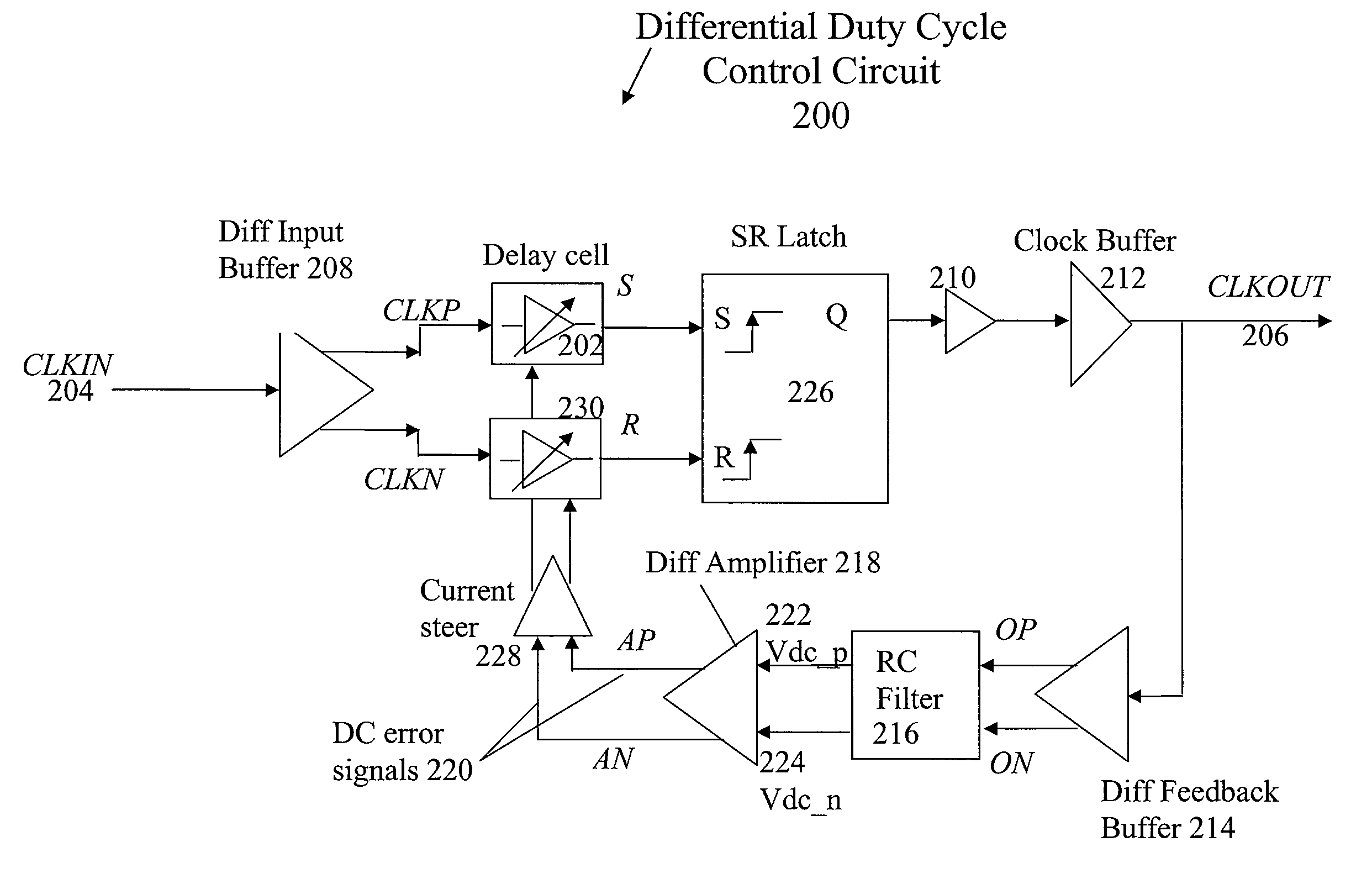
[0018]FIG. 3 shows a differential duty cycle correction (DDCC) circuit 200 according to one preferred embodiment of the present invention. The DDCC circuit 200 includes a differential input buffer 208 that receives an input clock signal 204. The input clock signal 204 can be a high speed clock signal with a frequency above 200 MHz. The differential buffer 202 converts the input clock signal 204 into two complementary differential input clock signals CLKP and CLKN. The differential input clock signals CLKP and CLKN are input into delay cells 202 and 230, respectively. The delay cells 202 and 230 introduce delays into the differential input clock signals CLKP and CLKN and output delayed differential input clock signals S and R, respectively. The delays introduced by the delay cells 202 and 230 are adjustable and are controlled by currents output from a current steer 228. The DDCC circuit 200 further includes an SR latch 226. The SR latch receives the delayed differential input clock s...


PUM


Abstract

The present invention implements an apparatus for correcting duty cycle distortion in high speed clock signals. The apparatus includes delay cells that delay each of first and second differential initial clock signals. The apparatus further includes a latch that generates an output clock signal based on the delayed first and second differential initial clock signals. The apparatus further includes a differential feedback buffer that converts the output clock signal into first and second differential feedback signals. The apparatus further includes a feedback circuit that adjusts the delay cells based on the first and second differential feedback signals.

Description

FIELD OF THE INVENTION[0001]The invention pertains to electronic circuits that use a high speed clock signal. More particularly, the invention pertains to a method and apparatus for correcting duty cycle distortion in a high speed clock signal in an electronic circuit.BACKGROUND OF THE INVENTION[0002]In electronic devices, a clock signal that oscillates from a high state to a low state is used to coordinate the timing of two or more electronic circuits. Several electronic circuits can be coordinated together by feeding a common clock signal to each of the several circuits, synchronizing the rising and falling edges of the clock signal at each circuit, and then coordinating the circuits' timing based on the rising and / or falling edges of the common clock signal. The relative timing of the rising and falling edges of a clock signal is referred to as a “duty cycle”. Typically, the rising edge and falling edge of a clock signal are separated by equal periods of time, resulting in a duty...

Claims


Application Information

Patent Timeline
Patent Type & Authority Patents(United States)
IPC IPC(8): H03K3/017
CPCH03K5/1565
Inventor GUO, CHUNBINGYANG, FUJI
Owner AVAGO TECH WIRELESS IP SINGAPORE PTE
Why Eureka
Try Eureka