Data read/write device

a data read/write and data technology, applied in nanoinformatics, instruments, record information storage, etc., can solve the problems of reducing the minimum line width, increasing processing costs, and limiting the recording density

Active Publication Date: 2010-06-08
KIOXIA CORP
View PDF22 Cites 23 Cited by
  • Summary
  • Abstract
  • Description
  • Claims
  • Application Information

AI Technical Summary

Problems solved by technology

However, in both of them, a limit of recording density has already been pointed out.
That is, there is a problem that an increase of processing cost caused by reduction of a minimum line width becomes remarkable in the NAND-type flash memory and tracking precision cannot be sufficiently allocated in a small sized HDD.
However, even up to now, such a MEMS memory capable of ferroelectric recording has not been achieved, although it is a conventionally known principle.
Namely, the electric field from the recording medium cannot be sensed, thus disabling a read operation.

Method used


Image

  • Data read/write device
  • Data read/write device
  • Data read/write device

Examples


first example

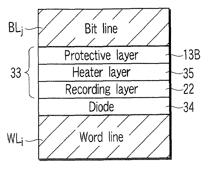
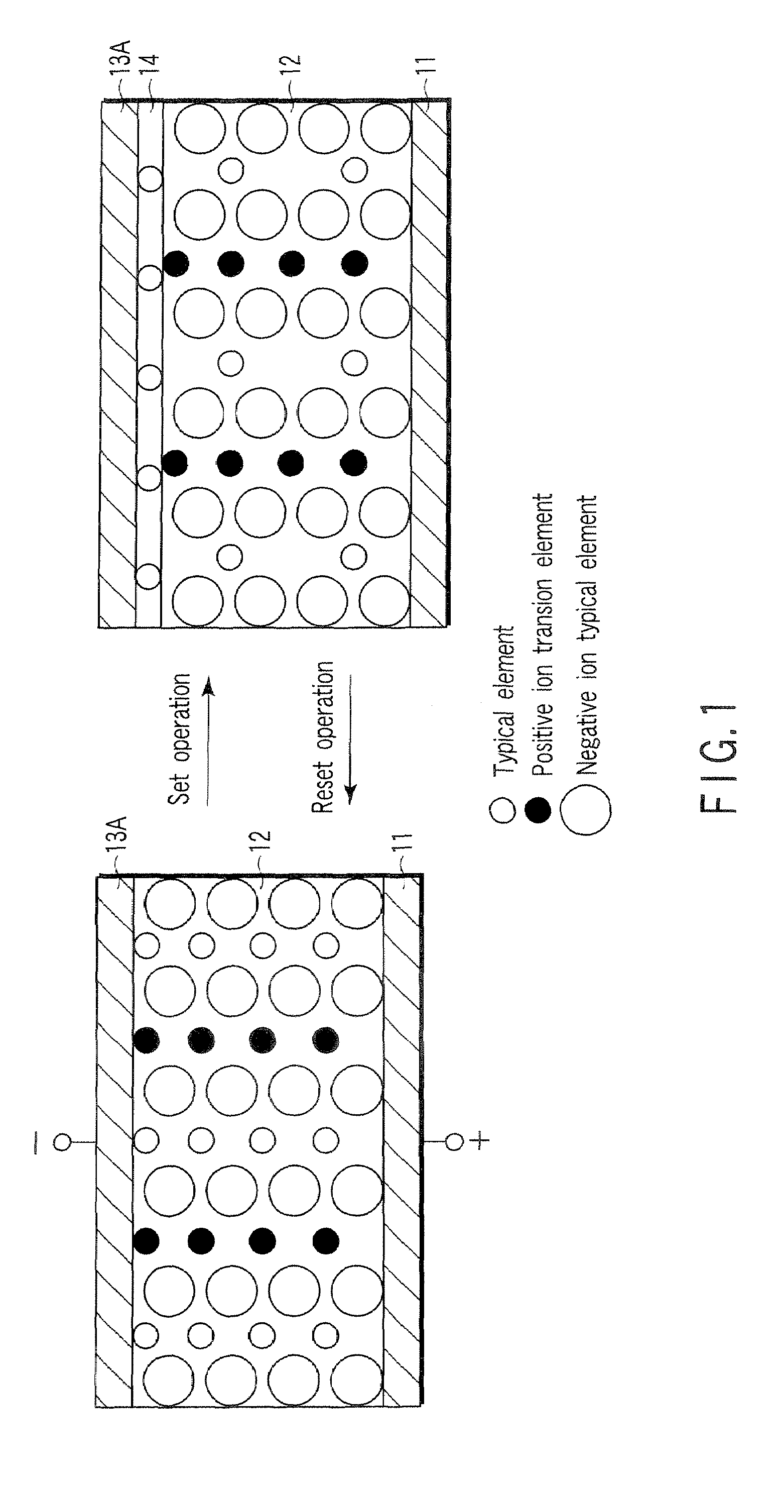
[0278]A first example shows a case of using the material shown in FIG. 1 for the recording layer.

[0279]A recording operation (set operation) may be achieved such that a voltage is applied to a selected memory cell 33, and a potential gradient is generated in the memory cell 33 to supply a current pulse. Thus, for example, a state in which a potential of a word line WLi is relatively lower than that of a bit line BLj is produced. Assuming that the bit line BLj is set at a fixed potential (for example, grounding potential), a negative potential may be applied to the word line WLi.

[0280]At this time, in the selected memory cell 33 enclosed by the dotted line A, some of positive ions move to the side of the word line (cathode) WLi, and the positive ions contained in crystal relatively decrease with respect to the negative ions. The positive ion having moved to the side of the word lines WLi precipitate as a metal upon the receipt of electrons from the word line WLi.

[0281]In the selected...

second example

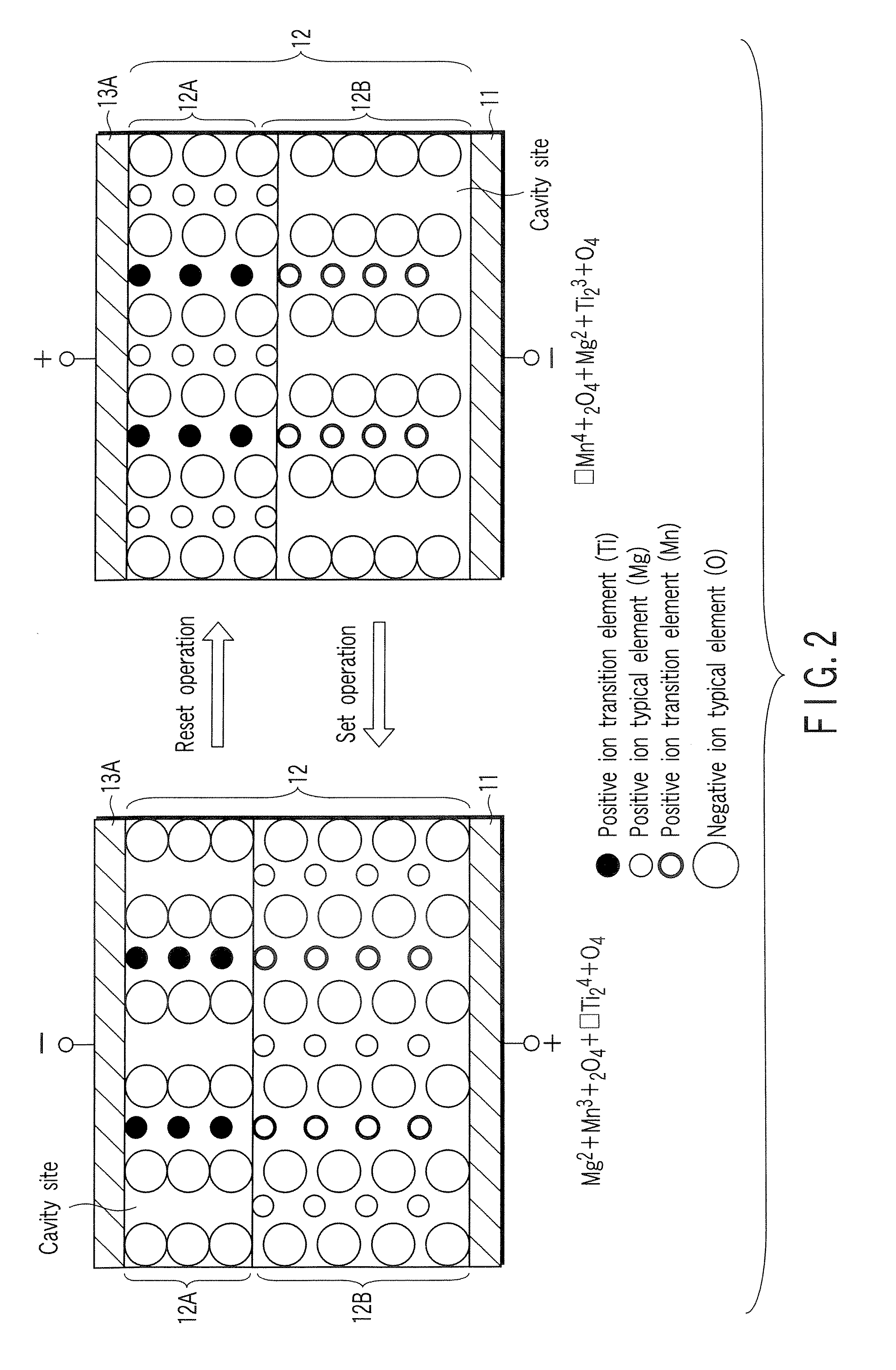
[0288]A second example shows a case of using the material shown in FIG. 2 for the recording layer.

[0289]In the write operation (set operation), a voltage is applied to the selected memory cell 33, whereby a current pulse may be supplied while an electric potential gradient is generated in that memory cell 33. Thus, for example, an electric potential of the word line WLi is relatively higher than that of the bit line BLj. A positive electric potential may be applied to the word line WLi, when the bit line BLj is defined as a fixed electric potential (for example, grounding electric potential).

[0290]At this time, in the selected memory cell 33 encoded by the dotted line A, part of the positive ion in a first compound moves into a cavity area of a second compound. Thus, the valence of the positive ion (transition element) in the first compound increases, and then, the valence of the positive ion (transition element) in the second compound decreases.

[0291]As a result, the memory cell 33...

ninth experiment example

(9) NINTH EXPERIMENT EXAMPLE

[0340]In a ninth experiment example, the same samples as those used in the first example are used except that a recording layer is made of CaCrnO4.

[0341]Resistance values after write / erasure operations were in order of 103 Ω / 107 Ω as in the first experiment example, and a resistance difference therebetween was about 104 Ω. It was verified that a sufficient margin could be allocated at the time of a read operation.


PUM


Abstract

A data read / write device according to an example of the present invention includes a recording layer, and means for applying a voltage to the recording layer, generating a resistance change in the recording layer, and recording data. The recording layer is composed of a composite compound having at least two types of cation elements, at least one type of the cation element is a transition element having a “d” orbit in which electrons have been incompletely filled, and the shortest distance between the adjacent cation elements is 0.32 nm or less.

Description

CROSS-REFERENCE TO RELATED APPLICATIONS[0001]This application is based upon and claims the benefit of priority from prior Japanese Patent Applications No. 2005-359301, filed Dec. 13, 2005; and No. 2006-236743, filed Aug. 31, 2006, the entire contents of both of which are incorporated herein by reference.BACKGROUND OF THE INVENTION[0002]1. Field of the Invention[0003]The present invention relates to a data read / write device having high recording density.[0004]2. Description of the Related Art[0005]In recent years, a small sized portable device has been prevalent worldwide. At the same time, with significant progress of a high-speed data transmission network, a demand for a small sized large capacity nonvolatile memory has rapidly increased. Among them, a NAND-type flash memory and a small sized hard disk drive (HDD) have made rapid progress in recording density, and a large market has been formed.[0006]However, in both of them, a limit of recording density has already been pointed ou...

Claims


Application Information

Patent Timeline
Patent Type & Authority Patents(United States)
IPC IPC(8): G11C11/00
CPCB82Y10/00H01L27/2481G11B9/149G11C13/0007G11C13/0009G11C13/003H01L45/085H01L45/1233H01L45/126H01L45/147H01L27/2409G11B9/04G11B11/08G11C2213/12G11C2213/55G11C2213/56G11C2213/71G11C2213/72G11C2213/75G11C2213/79H10B63/84H10B63/20H10N70/245H10N70/8413H10N70/8836H10N70/826G11C13/02G11C5/14
Inventor KUBO, KOICHIHIRAI, TAKAHIROAOKI, SHINYACARTER, ROBINKAMATA, CHIKAYOSHI
Owner KIOXIA CORP
Why Eureka
Try Eureka