Method using a carrier for manufacturing a memory device and manufacturing method of a memory device using the same and memory device using the same

a memory device and carrier technology, applied in the direction of final product manufacturing, printed circuit aspects, instruments, etc., can solve the problems of reducing the size of the memory die in the memory card, reducing the yield rate, and reducing the size of the memory card. , to achieve the effect of significantly enhancing the yield rate and efficient overcoming the bowing problem

Active Publication Date: 2010-06-15
PHISON ELECTRONICS
View PDF5 Cites 0 Cited by
  • Summary
  • Abstract
  • Description
  • Claims
  • Application Information

AI Technical Summary

Benefits of technology

[0012]The present invention is directed to a carrier for manufacturing a memory device, a method using the same, and a portable memory device using the manufacturing method, capable of efficiently overcoming the bowing problem of the PCB and significantly enhancing the yield rate.
[0013]The present invention is directed to a carrier for manufacturing a memory device, a method using the same, and a portable memory device using the manufacturing method, capable of efficiently solving the problems that, during an SMT process, the pieces cannot be assembled successfully, an integrated circuit (IC) to be adhered is offset, or empty soldering or a short circuit occurs, so as to greatly enhance the yield rate.
[0014]The present invention provides a carrier for manufacturing a memory device, which includes a bottom plate, an intermediate cover, and a top cover. A PCB is placed and fixed on the bottom plate, which is used for forming a plurality of memory elements. The intermediate cover is used to press peripheral regions of the PCB and to expose regions where the memory elements are formed on the PCB, such that the PCB may be closely attached to the surface of the bottom plate by fixing the intermediate cover. The top cover is used to cover the memory elements formed on the PCB, and the memory elements are clamped by an external force, so as to protect the memory elements from being affected by the PCB due to thermal stress deformation.

Problems solved by technology

Therefore, the products manufactured by using the electronic integrated circuit gradually becomes light, thin, short, and small, such as electronic dictionaries, digital cameras, and various other digital products.
However, as the size of the memory card is increasingly reduced, the size of the memory dies in the memory card is also reduced accordingly, and the used printed circuit board also becomes much thinner and smaller.
If such a specification is adopted, during the process of manufacturing the memory cards, PCB manufacturers cannot overcome the problem of the bending of the PCB, i.e., the bowing problem in the field, which also causes the problem that the components cannot be installed successfully by using the Surface Mounted Technology (SMT), or deformation occurs during the reflow process.
Accordingly, the problem of empty soldering occurs during a soldering process, and as a result, the flash memory may suffer a short circuit problem.
Some PCB manufacturers have suggested amending the layout of the PCB to connect the plate edges, i.e., through the manner of the edge connector of gold fingers, which however cannot overcome the aforementioned problems, so the yield rate cannot be enhanced efficiently.
However, the conventional method is merely to add the top cover in the reflow process, which can only avoid thermal deformation occurring in the reflow process, but cannot overcome the bowing problem that has already occurred before the material of the PCB is purchased.
Therefore, the two-piece manufacturing carrier only may enhance the yield rate by 10%-15%, but the additional operation steps wastes some extra working hours.

Method used


Image

  • Method using a carrier for manufacturing a memory device and manufacturing method of a memory device using the same and memory device using the same
  • Method using a carrier for manufacturing a memory device and manufacturing method of a memory device using the same and memory device using the same
  • Method using a carrier for manufacturing a memory device and manufacturing method of a memory device using the same and memory device using the same

Examples


Embodiment Construction

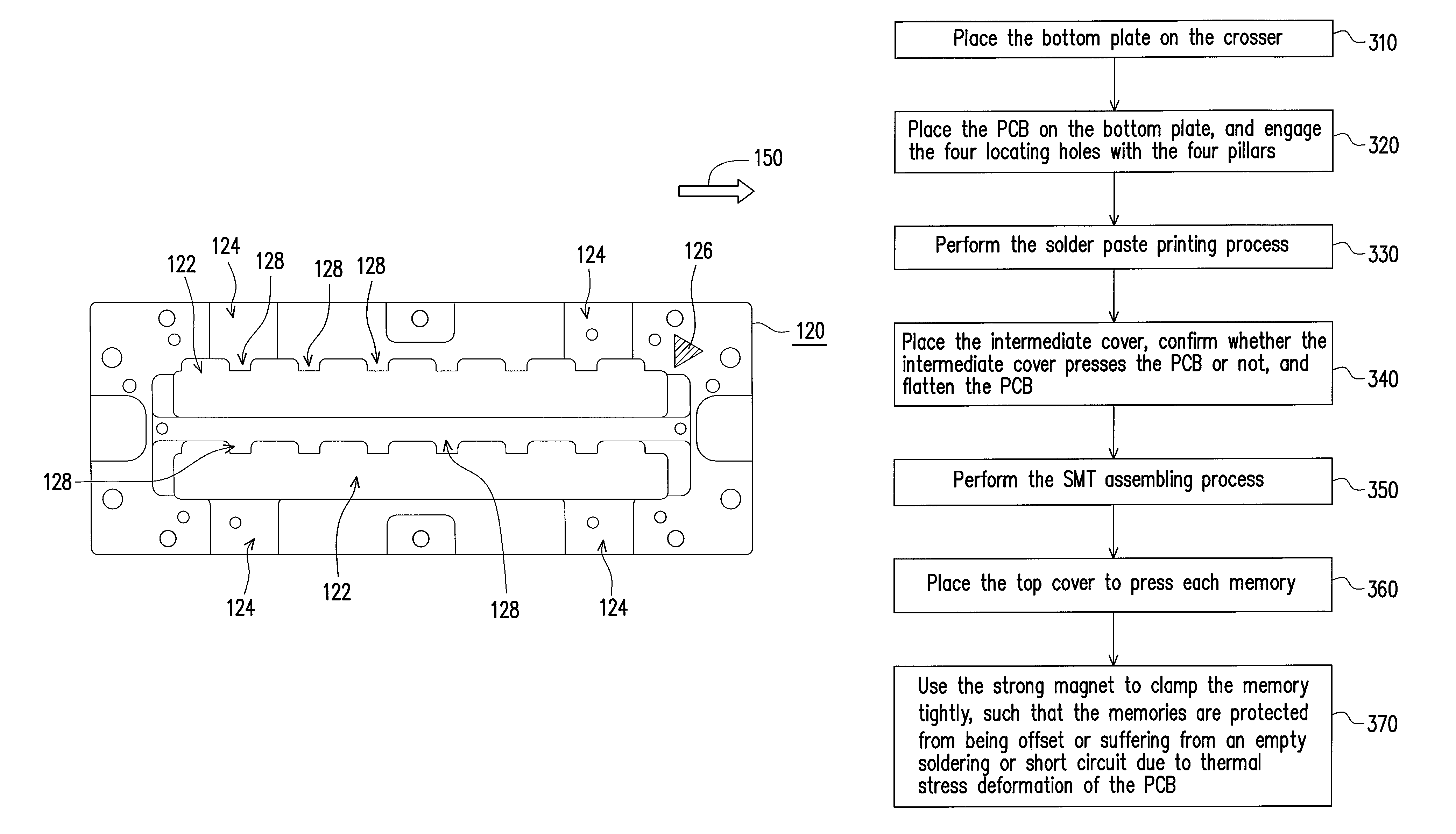
[0023]The carrier for manufacturing a memory device, the method using the same, and the portable memory device using the manufacturing method provided by the present invention is capable of efficiently overcoming the bowing problem of the printed circuit board (PCB) and also efficiently solving the problems that, during a surface mounted technology (SMT) process, pieces cannot be assembled successfully, an integrated circuit (IC) to be adhered is offset, or the empty soldering or short circuit problem occurs, so as to greatly enhance the yield rate of the manufacturing process.

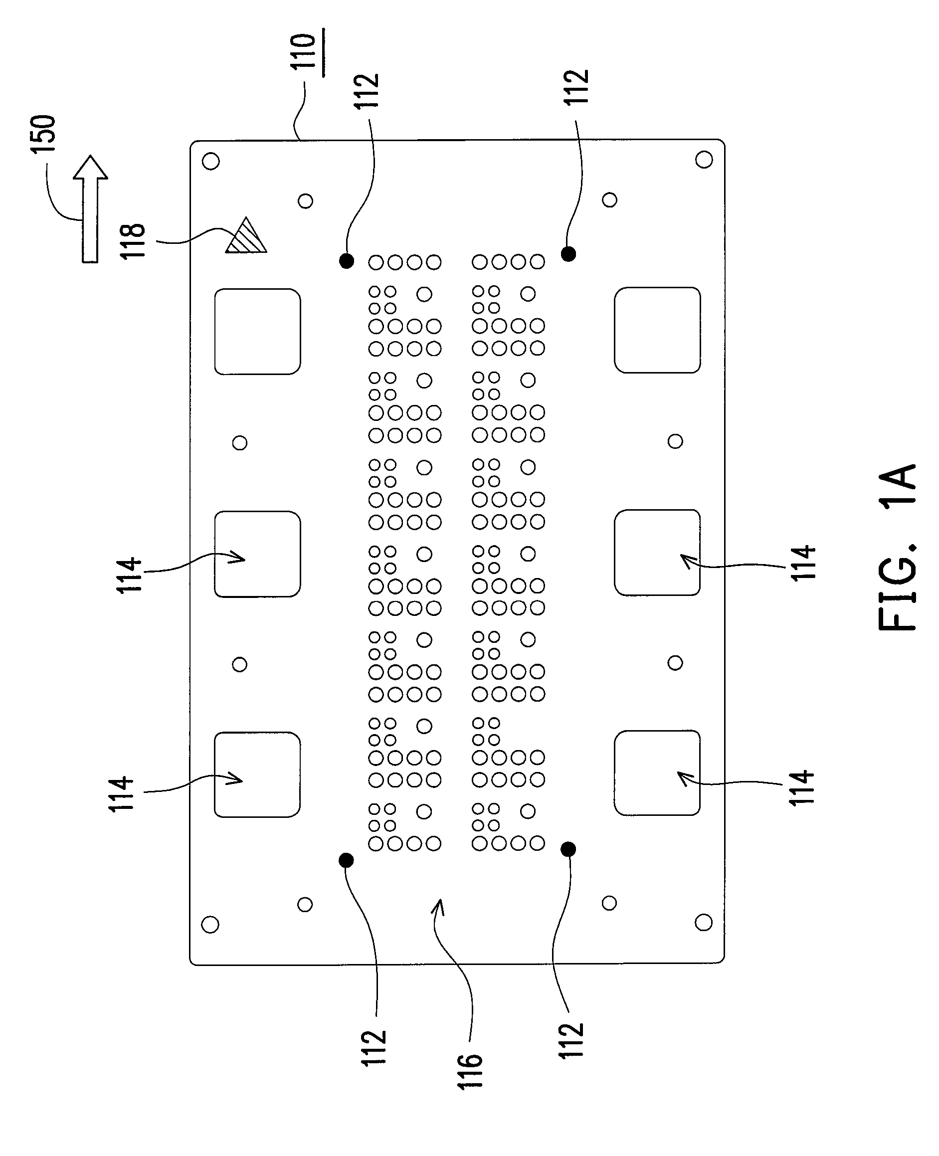
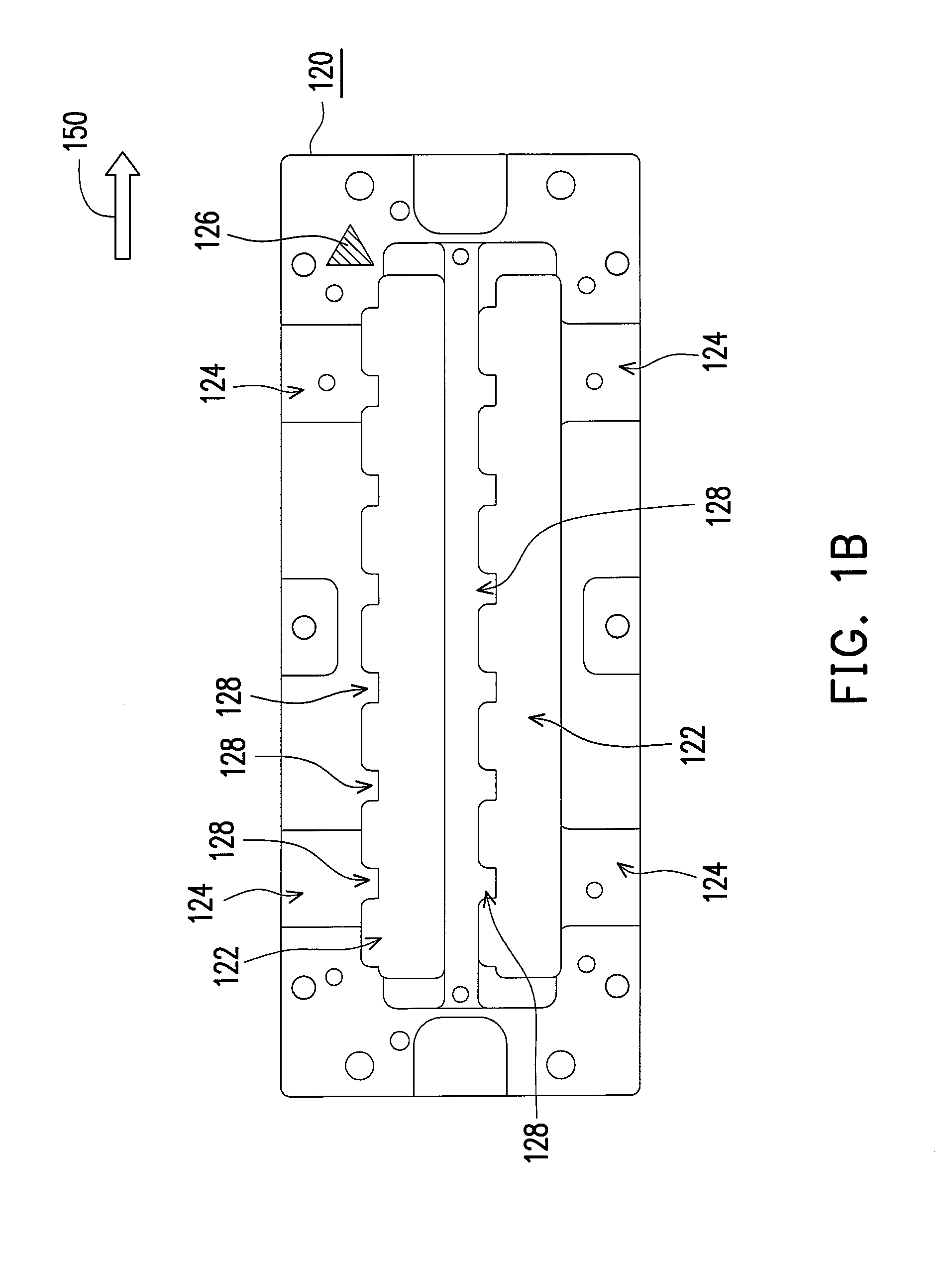
[0024]The carrier for manufacturing a memory device provided by the present invention is a three-piece carrier, which includes a bottom plate, an intermediate cover, and a top cover. FIGS. 1A, 1B, and 1C are schematic top views of the bottom plate, the intermediate cover, and the top cover, and FIGS. 2A, 2B, and 2C are side views of the bottom plate, the intermediate cover, and the top cover. In order to illus...


PUM

PropertyMeasurementUnit
thicknessaaaaaaaaaa
widthaaaaaaaaaa
lengthaaaaaaaaaa

Abstract

A carrier including a bottom plate, an intermediate cover, and a top cover for manufacturing a memory device is introduced herein. A printed circuit board is disposed on the bottom plate, and memory elements are arranged and disposed on the PCB. The intermediate cover is used to press peripheral regions of the printed circuit board, and to expose the regions where the memory elements are formed on the printed circuit board. The printed circuit board is closely attached to a surface of the bottom plate by fixing the intermediate cover. The top cover is used to cover the memory elements formed on the printed circuit board after some manufacturing processes, and by exerting an external force, the formed memory elements are clamped down, so as to protect the memory elements from being affected by the printed circuit board in the following thermal process due to the thermal stress deformation.

Description

CROSS-REFERENCE TO RELATED APPLICATION[0001]This application claims the priority benefit of Taiwan application serial no. 96113187, filed on Apr. 14, 2007. All disclosure of the Taiwan application is incorporated herein by reference.BACKGROUND OF THE INVENTION[0002]1. Field of the Invention[0003]The present invention relates to a carrier for manufacturing a memory device, a method using the same, and a portable memory device using the manufacturing method.[0004]2. Description of Related Art[0005]In recent years, the technology and material of an electronic integrated circuit have been developed rapidly, and the volume of a chip is increasingly reduced, but the function becomes increasingly powerful and the applications thereof have been gradually reached anywhere. Therefore, the products manufactured by using the electronic integrated circuit gradually becomes light, thin, short, and small, such as electronic dictionaries, digital cameras, and various other digital products. Further...

Claims


Application Information

Patent Timeline
Patent Type & Authority Patents(United States)
IPC IPC(8): H01L21/44H01L21/48H01L21/50
CPCH05K3/303H05K3/341H05K3/3484H05K3/3494H05K2201/09136Y10T29/4913H05K2203/0165H05K2203/0278H05K2203/104H05K2203/167Y10T29/49146H05K2201/10159H05K3/3485Y02P70/50
Inventor LIU, CHAO-TE
Owner PHISON ELECTRONICS
Why Eureka
Try Eureka