
Method for manufacturing semiconductor device

a manufacturing method and semiconductor technology, applied in the direction of semiconductor devices, electrical apparatus, transistors, etc., can solve the problems of low electrical conductivity of n-type sas, and achieve the effects of reducing cost, improving reliability, and simplifying a crystallization step

Inactive Publication Date: 2005-01-20
SEMICON ENERGY LAB CO LTD
View PDF25 Cites 73 Cited by
  • Summary
  • Abstract
  • Description
  • Claims
  • Application Information

AI Technical Summary

Benefits of technology

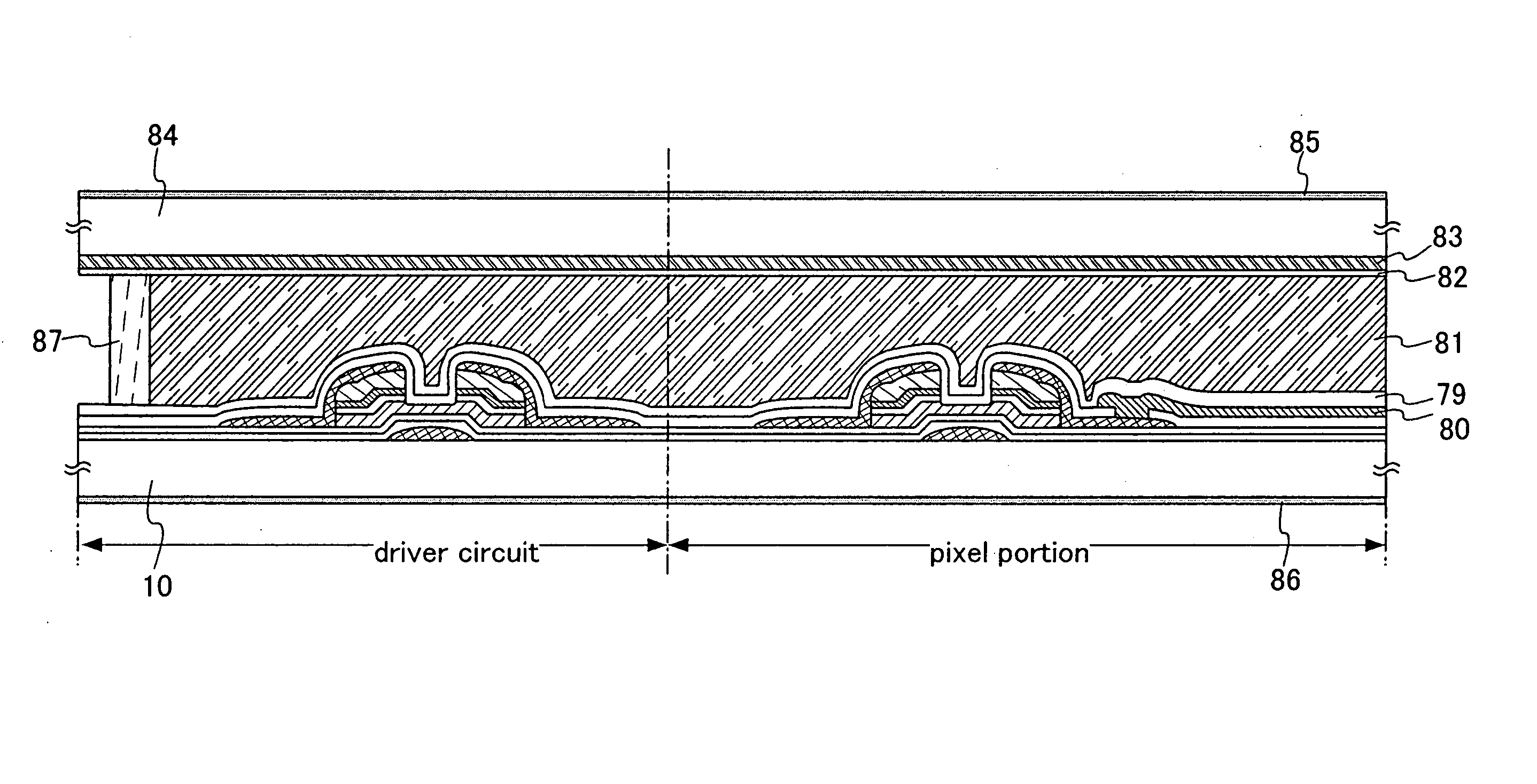
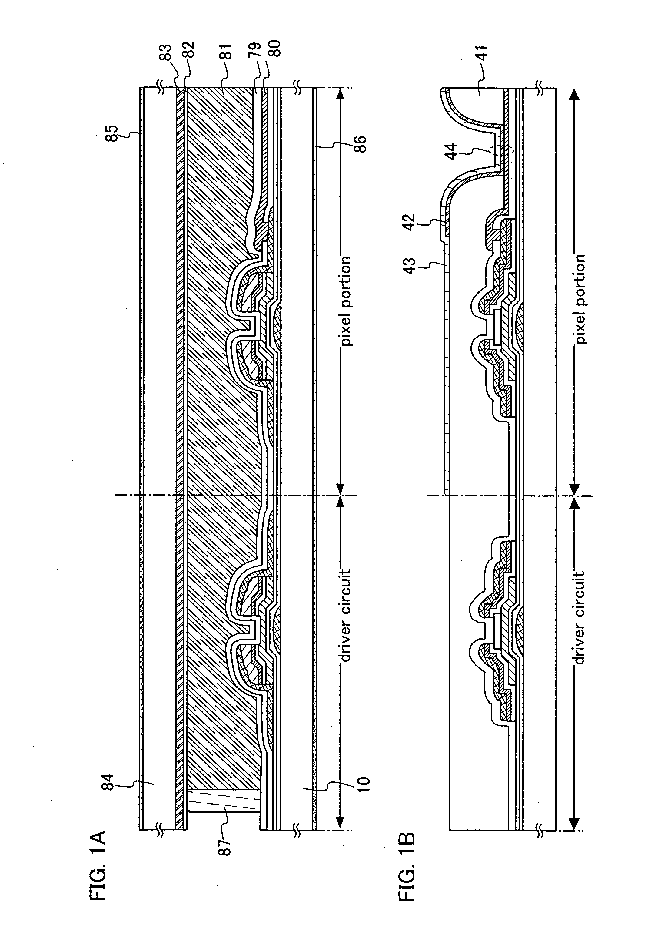
[0009] In view of the above problem, an object of the present invention is to provide a method for manufacturing a semiconductor device of which manufacturing process is simplified by improving a usage rate of a material, and a method for manufacturing a semiconductor device with which saving of manufacturing time and reduction of a manufacturing cost are realized.
[0014] The above SAS differs from a polycrystalline semiconductor, which can be formed directly on a substrate as a SAS. Specifically, the SAS can be formed using plasma CVD by diluting SiH4 with H2 in flow rate of 2 to 1000 times, preferably in flow rate of 10 to 100 times. The SAS that is manufactured using the above method also includes a microcrystal semiconductor containing a crystal grain of 0.5 nm to 20 nm in an amorphous semiconductor. Therefore, there is no necessity to provide a crystallization step after forming a semiconductor, which differs from the case where a polycrystalline semiconductor is used. In addition, although there is a limitation on a length of a major axis of a laser beam in the case of crystallization using laser light, there is no limitation on a size of a substrate in the case of SAS. In other words, it is possible to manufacture easily the SAS over a substrate in which one side of so-called 5 generations is a meter angle. In addition, the number of steps of manufacturing a transistor can be reduced, which alternatively can increase a yield rate of a display device and can control the cost. In the invention, a SAS may be at least used for a channel formation region. In addition, all parts in a direction of the film thickness of a channel formation region does not need to be a semi-amorphous semiconductor, but a semi-amorphous semiconductor may be included at least in a part thereof.
[0020] It is preferable that these driver ICs mounted on the first substrate are formed of a crystalline semiconductor layer. The crystalline semiconductor layer is preferable to be formed by being irradiated with continuous-wave laser. Therefore, a solid state laser or a gas laser of continuous-wave laser is used as an oscillator in which the laser light is generated. There is few crystal defects when a continuous-wave laser is used, which is as a result that a transistor can be manufactured by using a polycrystalline semiconductor layer with a large grain size. Furthermore, since mobility and a response speed are favorable, a high-speed drive is possible, which makes possible to further improve an operating frequency of an element than conventional, so that high reliability can be obtained since there is few properties variations. In addition, a channel-length direction of a transistor and a scanning direction of laser light may be accorded with each other to further improve a frequency in an operation.
[0026] The invention can provide a method for manufacturing a thin film transistor and a display device having electron field-effect mobility of 2 to 10 cm2 / V·sec which is improved than a transistor using an amorphous semiconductor by composing a channel formation region with a semi-amorphous semiconductor. Therefore, it becomes possible to simplify a step of crystallization and to use this transistor as a switching element of a pixel, and further to use not only as a switching element of a pixel but also as an element that forms a scanning line (gate line) driver circuit. Consequently, a display device that realizes a system-on-panel can be manufactured. In addition, in the invention, it becomes possible to form a thin film transistor without using a resist mask at all or just with a few by using a droplet discharge method. Therefore, steps such as applying a resist, baking a resist, light exposure, developing, baking after developing, or peeling of a resist can be eliminated, so that great decrease of cost or increase of reliability due to simplification of the steps can be realized.
[0027] The invention having the above structure makes possible to provide a method for manufacturing a thin film transistor and a display device, which simplifies a manufacturing step by improving a usage rate of materials and to provide a method for manufacturing a thin film transistor and a display device that realized saving manufacturing time and reducing a manufacturing cost.

Problems solved by technology

In addition, a SAS shows low electrical conductivity of n-type when an impurity element to control a valence electron is not doped intentionally.

Method used


Image

  • Method for manufacturing semiconductor device
  • Method for manufacturing semiconductor device
  • Method for manufacturing semiconductor device

Examples


example

[0155] In this example, a method for mounting a driver IC will be described with reference to FIGS. 8A to 8E. The driver IC may be mounted by connection using an anisotropic conductive material, by wire bonding, and the like. An example of the mounting methods is explained with reference to FIGS. 8A to 8E.

[0156] Explanation is made on an example of a driver IC 208 mounted on a first substrate 201 by using an anisotropic conductive material. A pixel region 202, a lead wiring 206, and connection wiring and an input-output terminal 207 are formed on the first substrate 201. A second substrate 203 is attached to the first substrate 201 with a sealant 204, and a liquid crystal layer 205 is interposed therebetween.

[0157] An FPC 212 is attached to one side of connection wiring and an input-output terminal 207 by using an anisotropic conductive material. The anisotropic conductive material comprises a resin 215 and conductive particles 214 having a surface plated with Au and the like and ...

example 2

[0164] In this example, a configuration of a display device of the present invention is briefly described. As mentioned above, a driver IC is used as a driver circuit of a liquid crystal display device or an EL display device. FIGS. 9A and 9B are block diagrams of such display device. A pixel region 1601 is formed of a plurality of scanning lines and data lines, which may be either in an active matrix type in which TFTs are provided or in a passive matrix type may be adopted. In the periphery of the pixel region 1601, a scanning line driver circuit 1602 and a data line driver circuit 1603 which correspond to driver ICs are disposed.

[0165] A clock signal, a start pulse 1607, and a video signal 1608 inputted from outside are inputted to a control circuit 1605 for converting to an input specification of the driver IC, and converted to each timing specification. A power supply 1609 and a is power supply circuit 1606 composed of an operation amplifier are externally provided. For the ef...

example 3

[0168] In this example, a configuration of a droplet discharge method is described with reference to FIGS. 10A and 10B. First, a droplet discharge device is described briefly with reference to FIG. 10A. A droplet discharge means equipped with a head in which a plurality of nozzles is arranged in a uniaxial direction (not shown), a controller and a CPU controlling the droplet discharge means (not shown), a stage 503 which fixes a substrate 501 and moves the substrate in a XYθ direction, and the like are given as indispensable components of this device. A fixator (a frame) in which the droplet discharge means is provided has a configuration in which the droplet discharge means shown in FIG. 10B is fixed. The stage 503 has a function to fix the substrate 501 with a vacuum chuck method or the like. Then, a pattern is formed on the substrate 501 by discharging a composition in a direction of the substrate 501 from discharge openings of each nozzle with the droplet discharge means.

[0169]...


PUM


Abstract

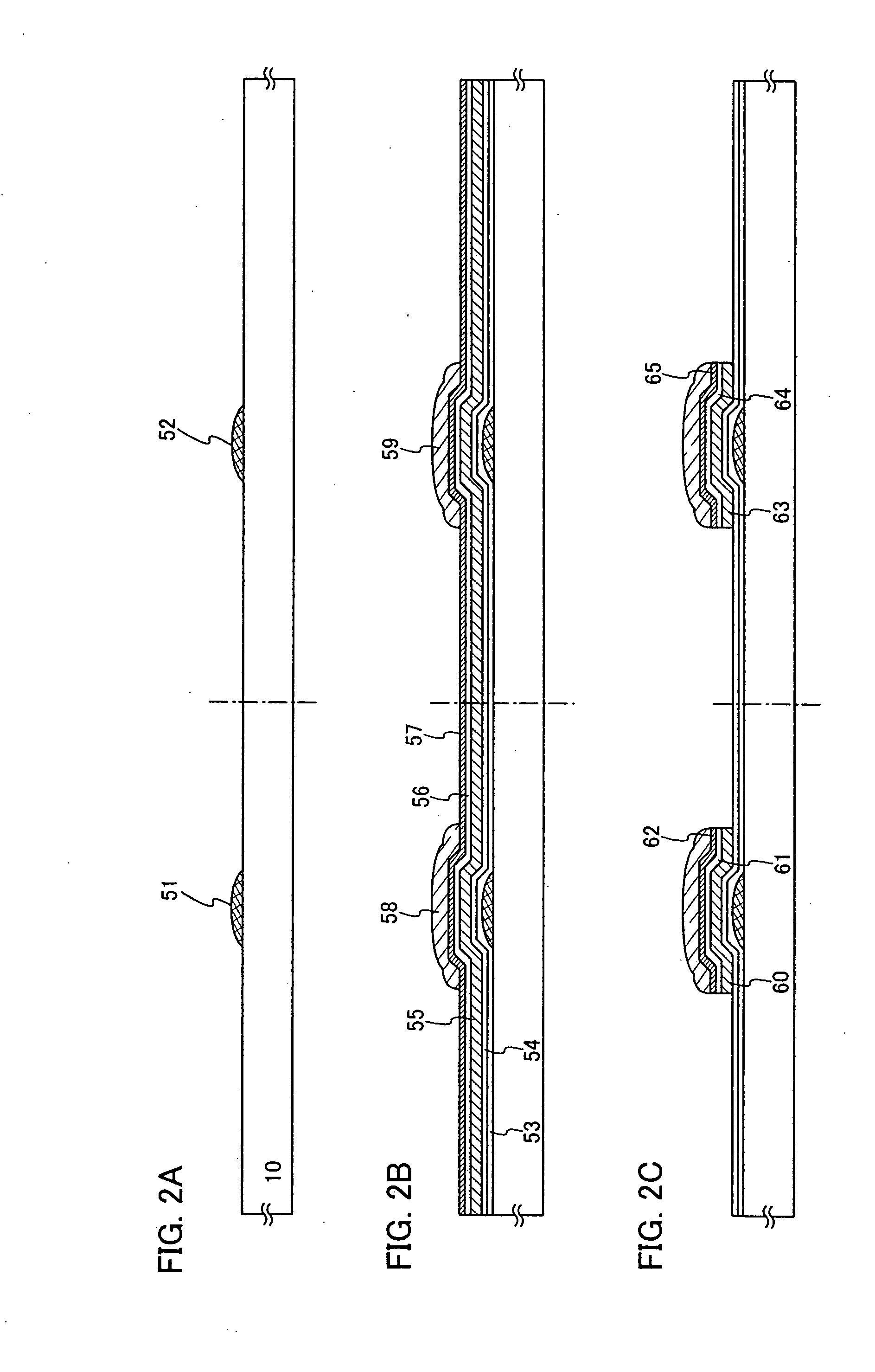
An object of the present invention is to provide a method for manufacturing a semiconductor device of which manufacturing process is simplified by improving usage rate of a material. A method for manufacturing a semiconductor device of the invention comprises the steps of: forming gate electrodes with a droplet discharge method on a substrate having an insulating surface; laminating gate insulating layers, semiconductor layers, and a semiconductor layer containing one-conductivity type impurity over the gate electrodes; forming first conductive layers serving as masks with a droplet discharge method in a position overlapping the gate electrodes, etching the semiconductor layer and the semiconductor layer containing one-conductivity type impurity with the first conductive layers, forming a second conductive layer serving as a source wiring or a drain wiring with a droplet discharge method over the first conductive layers; and etching the first conductive layers and the semiconductor layer containing one-conductivity type impurity, using the second conductive layers as masks.

Description

BACKGROUND OF THE INVENTION [0001] 1. Field of the Invention [0002] The present invention relates to a method for manufacturing a thin film transistor with the use of a droplet discharge method, and to a method for manufacturing a display device equipped with the thin film transistor. [0003] The invention relates to a method for manufacturing a semiconductor device with the use of a droplet discharge method. [0004] 2. Description of the Related Art [0005] In recent years, pattern formation by a droplet discharge method (ink-jet printing) is applied to a field of a flat panel display, of which development is actively carried out. The droplet discharge method has a lot of advantages that a mask is unnecessary due to direct drawing, of applicability to a large-scaled substrate, of high a usage rate of materials, and the like; therefore, the droplet discharge method is applied for manufacturing an EL layer or a color filter, an electrode of a plasma display, and the like. [0006] [Non-Pa...

Claims


Application Information

Patent Timeline
Patent Type & Authority Applications(United States)
IPC IPC(8): H01L21/336H01L21/77H01L21/84H01L29/786H01L27/12H01L29/423
CPCH01L27/12H01L27/1292H01L29/66765H01L29/42384H01L21/288H01L27/1214
Inventor YAMAZAKI, SHUNPEIIMAI, KEITAROMAEKAWA, SHINJIFURUNO, MAKOTONAKAMURA, OSAMU
Owner SEMICON ENERGY LAB CO LTD
Learn More