

Metal-gate CMOS device
a metal-gate, cmos technology, applied in the direction of semiconductor devices, electrical devices, transistors, etc., can solve the problems of increasing difficulty, requiring a much stricter demand, and reducing the complexity of cmos fabrication steps, so as to reduce the manufacturing cost and simplify the manufacturing process
- Summary
- Abstract
- Description
- Claims
- Application Information
AI Technical Summary
Benefits of technology
Problems solved by technology
Method used
Image

Examples
Embodiment Construction
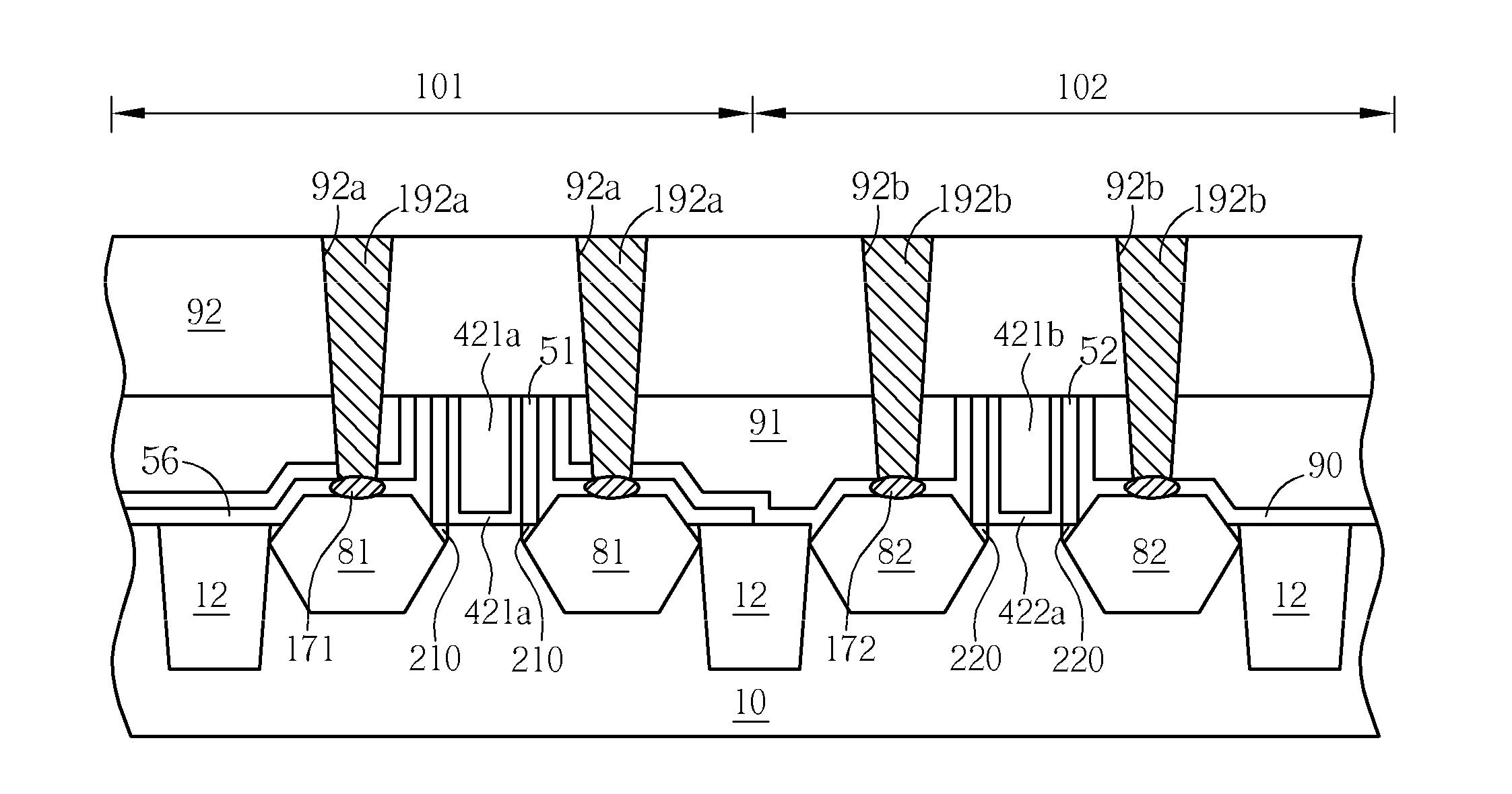
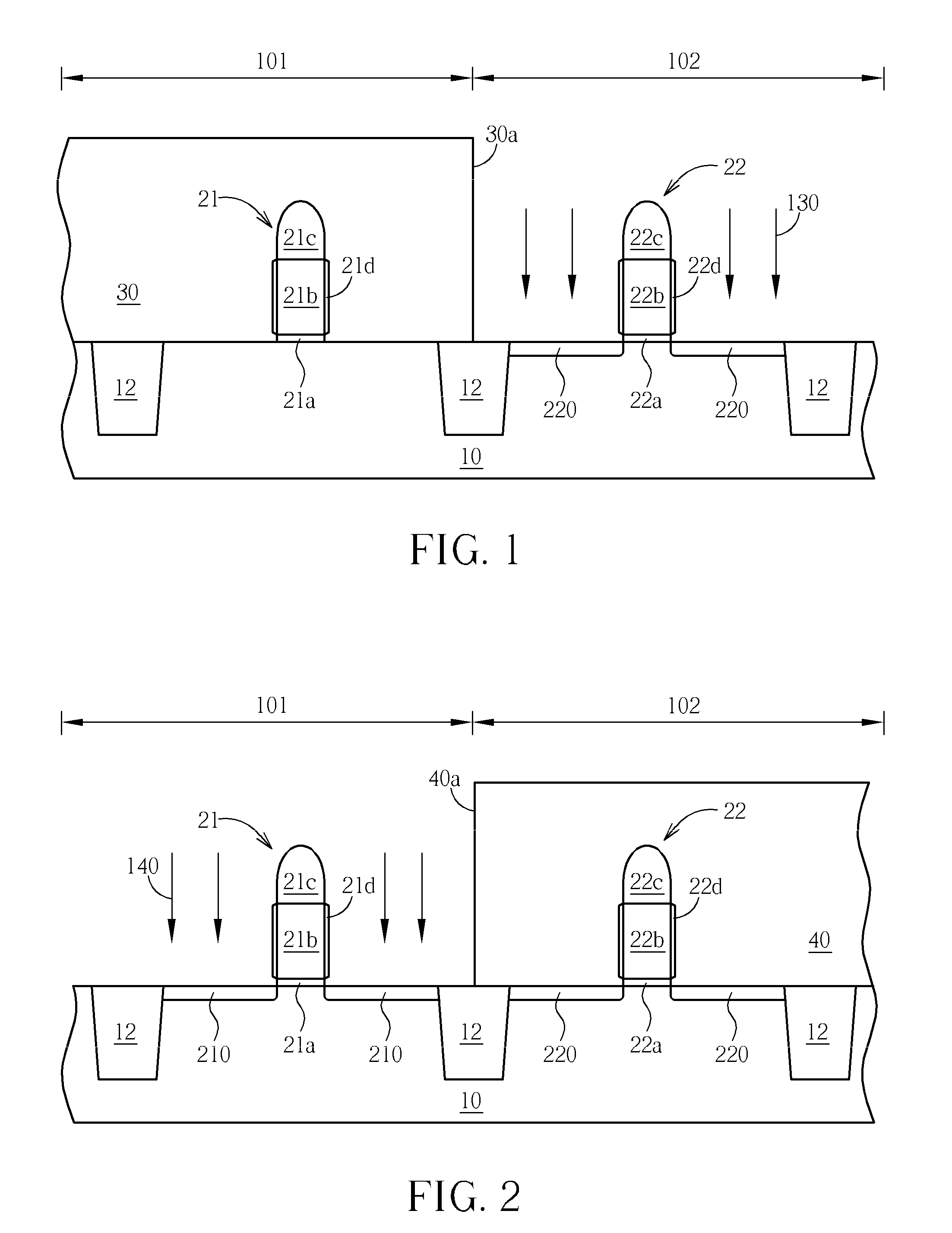
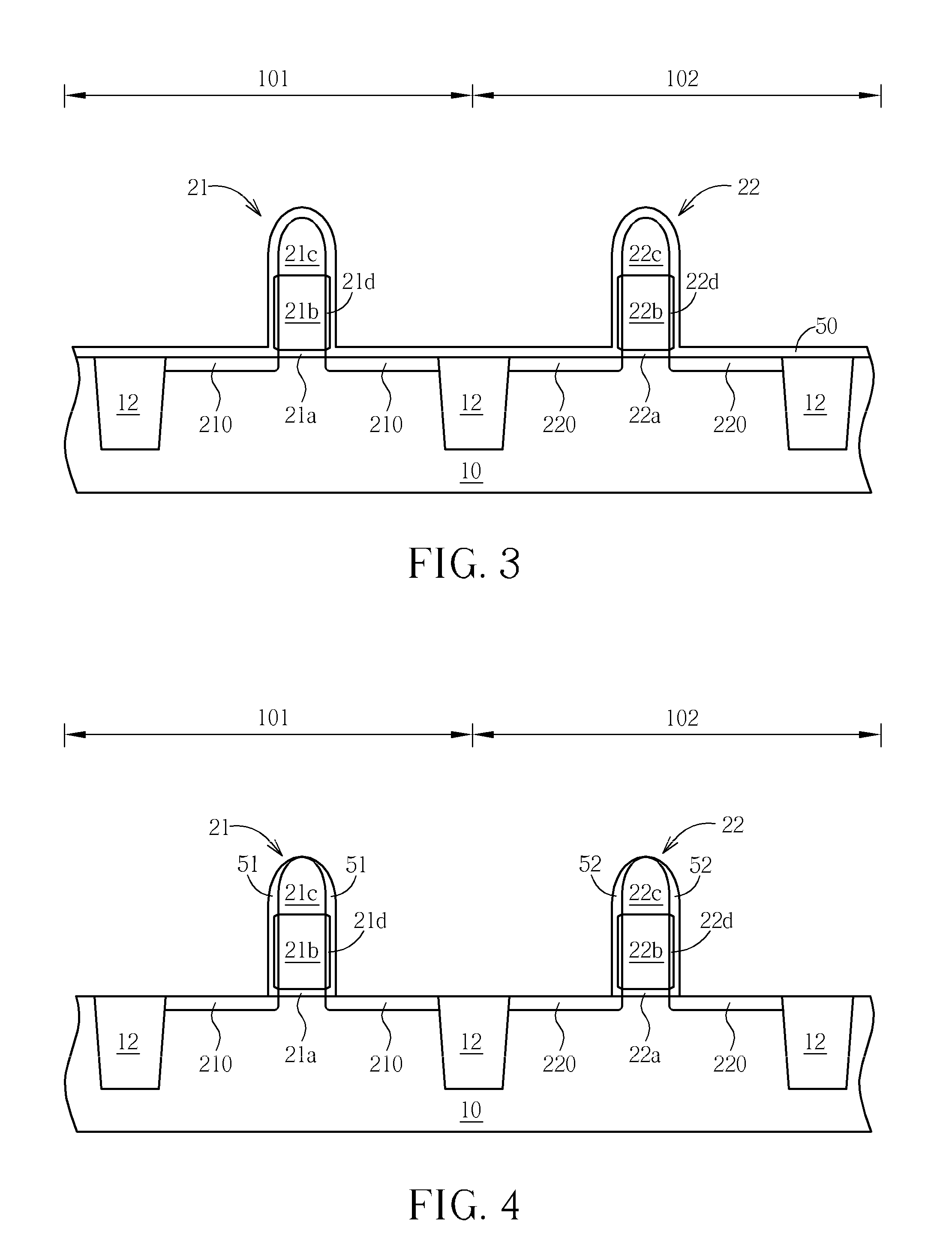
[0017]Please refer to FIG. 1 to FIG. 14. FIG. 1 to FIG. 14 are schematic, cross-sectional diagrams showing a method for fabricating a dual work-function CMOS device in accordance with one preferred embodiment of this invention. As shown in FIG. 1, a substrate 10 such as silicon substrate, silicon-containing substrate, silicon-on-insulator (SOI) substrate or epitaxial substrate is provided. A plurality of shallow trench isolation (STI) structures 12 are provided in the main surface of the substrate 10 to electrically isolate at least one PMOS region 101 and at least one NMOS region 102. Subsequently, a dummy gate structure 21 and a dummy gate structure 22 are formed on the substrate 10 within the PMOS region 101 and the NMOS region 102 respectively. The dummy gate structure 21 may comprise a gate oxide layer 21a, a polysilicon layer 21b, a cap layer 21c and a sidewall oxide layer 21d. The dummy gate structure 22 may comprise a gate oxide layer 22a, a polysilicon layer 22b, a cap laye...
PUM
 Abstract
Description
Claims
Application Information