
Semiconductor device and fabrication method thereof

a technology of semiconductors and semiconductors, applied in the direction of semiconductor devices, electrical devices, transistors, etc., can solve the problems of difficult to provide electrical properties capable of meeting requests, and achieve the effect of simplifying the steps of fabricating

Inactive Publication Date: 2005-05-03
SEMICON ENERGY LAB CO LTD
View PDF19 Cites 74 Cited by
  • Summary
  • Abstract
  • Description
  • Claims
  • Application Information

AI Technical Summary

Benefits of technology

[0009]One of the objects of the present invention is to provide a technology for fabricating a bottom gate type TFT by steps having high mass production performance.
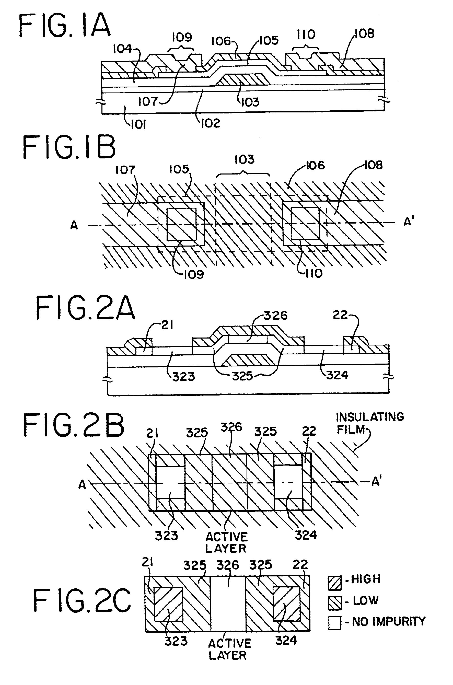
[0017]Further, in the step of patterning the insulating silicon film in the above-described constitution, sometimes the insulating silicon film remains at the end portions of the active layer so as to cover the end portions. As discussed infra, the constitution wherein the insulating silicon film remains at the end portions of the active layer in this way, significantly contributes to simplifying the steps of fabricating TFT.

Problems solved by technology

However, the carrier mobility of amorphous silicon is small, and accordingly, requested electric properties are provided by enlarging the size of the individual TFT.
Situations in which electric properties capable of meeting the request are very difficult to provide in the case of amorphous silicon.

Method used


Image

  • Semiconductor device and fabrication method thereof
  • Semiconductor device and fabrication method thereof
  • Semiconductor device and fabrication method thereof

Examples


embodiment 6

[Embodiment 6]

[0091]In this embodiment, an explanation will be given of an example in the case where an active matrix type LCD is constituted by using an active matrix substrate having a constitution shown by Embodiments 1 through 5. FIGS. 6A and 6B show the externals of the active matrix type LCD according to the embodiment.

[0092]In FIG. 6A, numeral 601 designates an active matrix substrate on which a pixel matrix circuit 602, a source driver circuit 603 and a gate driver circuit 604 are constituted by TFTs according to the present invention. Further, numeral 605 designates an opposed substrate.

[0093]In the active matrix type LCD of the embodiment, end faces of the active matrix substrate 601 and the opposed substrate 605 are aligned and pasted together. However, only a portion of the opposed substrate 605 is removed and a FPC (Flexible Print Circuit) 606 is connected to an exposed portion of the active matrix substrate. By the FPC 606, an outside signal is transmitted into the inn...

embodiment 8

[Embodiment 8]

[0106]The active matrix type LCDs shown by Embodiments 6 and 7 are utilized as displays of various electronic devices. Further, an electronic device according for the embodiment is defined as a product mounted with an electrooptical device represented by an active matrix type LCD.

[0107]Such electronic devices, include a video camera, a still camera, a projector, a projection TV, a head mount display, a car navigation system, a personal computer (including notebook type), a portable information terminal (mobile computer, portable telephone or the like). Examples of these are shown in FIGS. 7A to 7F.

[0108]FIG. 7A shows a portable telephone which is constituted by a main body 2001, a sound outputting unit 2002, a sound inputting unit 2003, a display device 2004, operation switches 2005 and an antenna 2006. The present invention is applicable to the display device 2004 and so on.

[0109]FIG. 7B shows a video camera which is constituted by a main body 2101, a display device 2...


PUM


Abstract

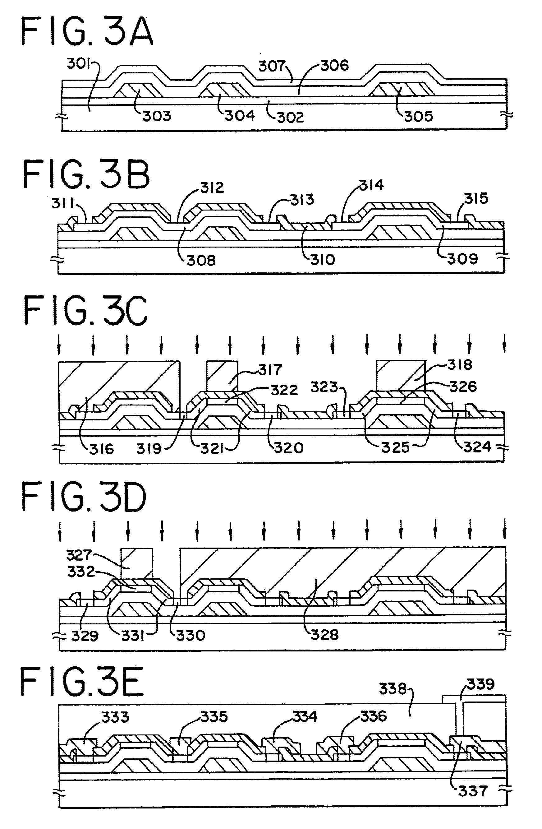
To provide a technology for fabricating a bottom gate type TFT by steps having high mass production performance, an insulating film whose major component is silicon is formed on an active layer, the insulating film is patterned and openings are formed at portions thereof constituting source and drain regions at later steps, a resist is provided right above a portion for forming a channel forming region at later steps, a step of adding an impurity is carried out and in this case, the patterned insulating film is utilized as a doping mask.

Description

BACKGROUND OF THE INVENTION[0001]1. Field of the Invention[0002]The present invention relates to a thin film transistor (hereinafter, abbreviated as TFT) of a bottom gate type which is fabricated by utilizing a semiconductor thin film.[0003]2. Description of Related Art[0004]Currently, a liquid crystal display device (hereinafter, abbreviated as LCD) is utilized as the display for notebook personal computers or portable information terminals. In the past, a passive type LCD was mainly used. However, with requests for highly fine images becoming more enhanced, an active matrix type LCD has become the main stream.[0005]An active matrix type LCD is provided with a plurality of TFTs arranged in a matrix in a display unit thereof. Voltage control is carried out at each pixel with a TFT as a switching element by which the desired image is realized. An inverted stagger type TFT using amorphous silicon for an active layer has been frequently utilized.[0006]For such an inverted stagger type ...

Claims


Application Information

Patent Timeline
Patent Type & Authority Patents(United States)
IPC IPC(8): H01L21/70H01L27/12H01L29/66H01L29/786H01L21/84H01L21/86H01L21/77H01L21/336
CPCH01L27/1214H01L29/78621H01L29/78678H01L29/78669H01L29/78684H01L27/127
Inventor NAKAJIMA, SETSUOFUKUNAGA, TAKESHI
Owner SEMICON ENERGY LAB CO LTD
Learn More