Method of fabricating the display device

a display device and manufacturing method technology, applied in the manufacture of final products, electric discharge tubes/lamps, discharge tubes luminescnet screens, etc., can solve the problems of precision and deflection of masks used in vapor deposition, and achieve high reliability, simplified steps, and high resolution

Inactive Publication Date: 2010-07-13
SEMICON ENERGY LAB CO LTD
View PDF24 Cites 78 Cited by
  • Summary
  • Abstract
  • Description
  • Claims
  • Application Information

AI Technical Summary

Benefits of technology

[0017]When using the invention, a display device with high reliability can be manufactured by simplified steps. Therefore, a display device with high resolution and high image quality can be manufactured at low cost with high yield.

Problems solved by technology

However, there is a problem in that a defect occurs due to a precision and a deflection of a mask used in vapor deposition which is caused by the fineness of a pixel region in accordance with higher resolution and the large size of a substrate in accordance with a larger area.

Method used


Image

  • Method of fabricating the display device
  • Method of fabricating the display device
  • Method of fabricating the display device

Examples


embodiment mode 1

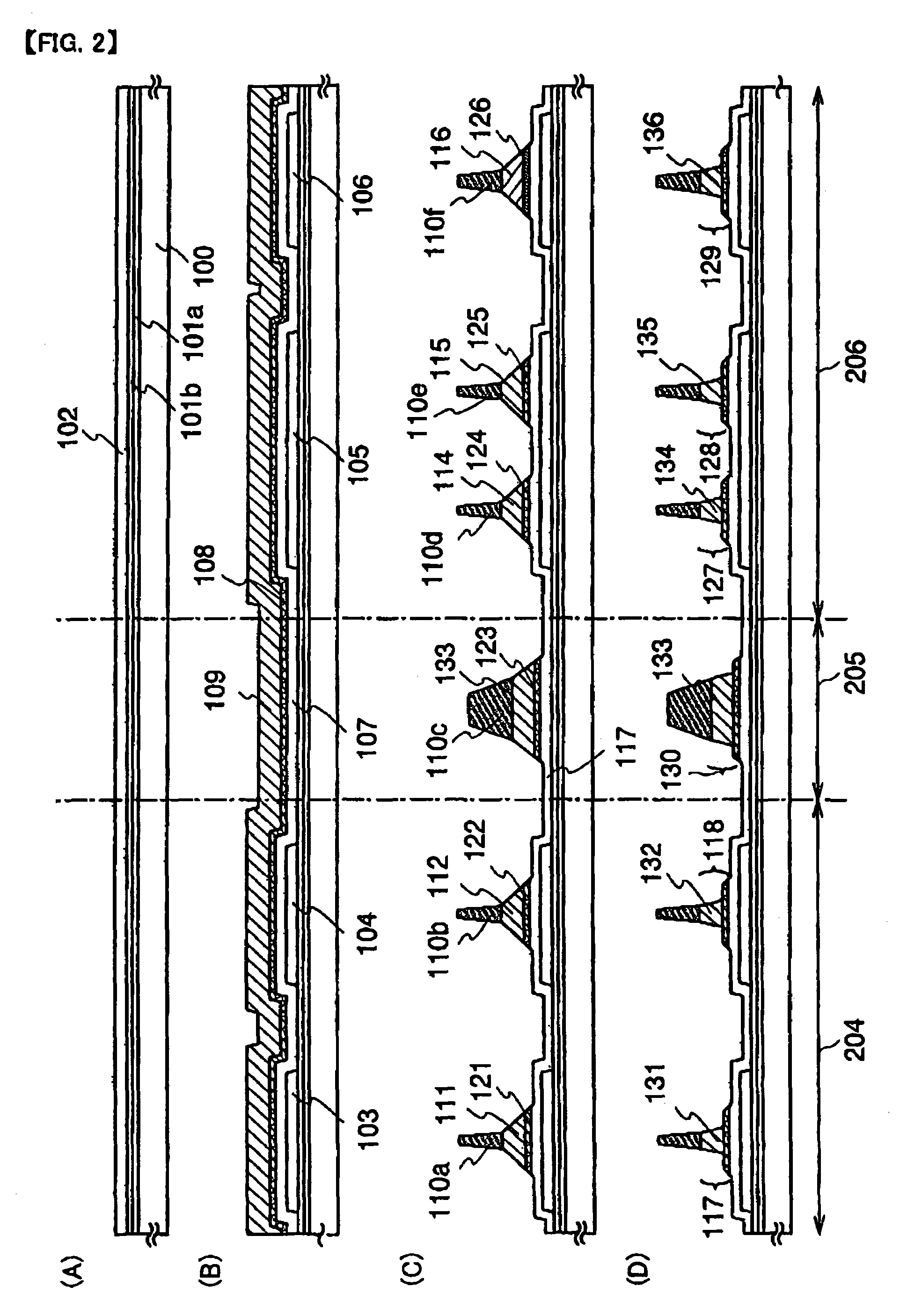
[0054]A method for manufacturing a thin film transistor of this embodiment mode is described in details with reference to FIGS. 1 to 6, 16 and 17.

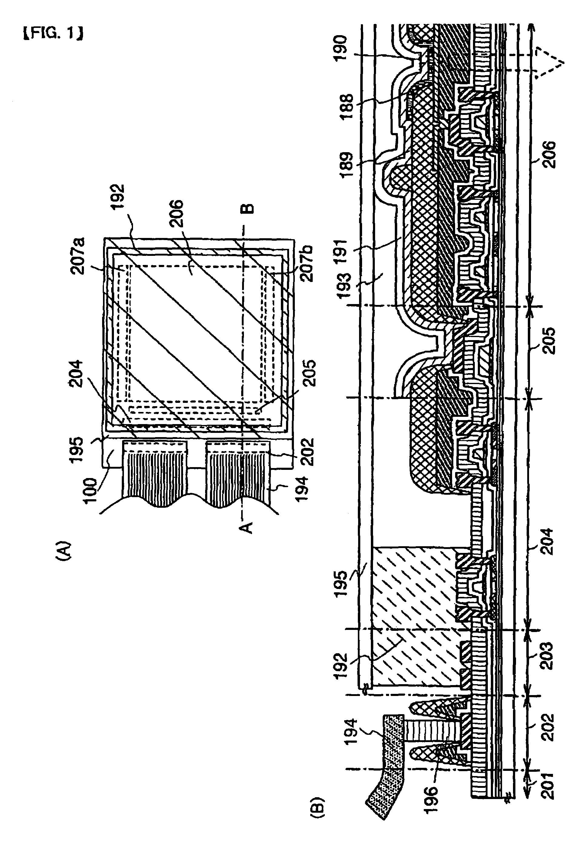
[0055]FIG. 16(A) is a top plan view showing a structure of a display panel in accordance with the invention, in which a pixel portion 2701 where pixels 2702 are arranged in matrix, a scan line side input terminal 2703, and a signal line side input terminal 2704 are formed over a substrate 2700 having an insulating surface. The number of pixels may be set in accordance with various standards, and 1024×768×3 (RGB) pixels may be provided in the case of XGA, 1600×1200×3 (RGB) pixels may be provided in the case of UXGA, and 1920×1080×3 (RGB) pixels may be provided in the case of corresponding to a full spec high vision.

[0056]Scan lines extending from the scan line side input terminal 2703 and signal lines extending from the signal line side input terminal 2704 cross each other so that the pixels 2702 are disposed in matrix. Each pixel 2702 is p...

embodiment mode 2

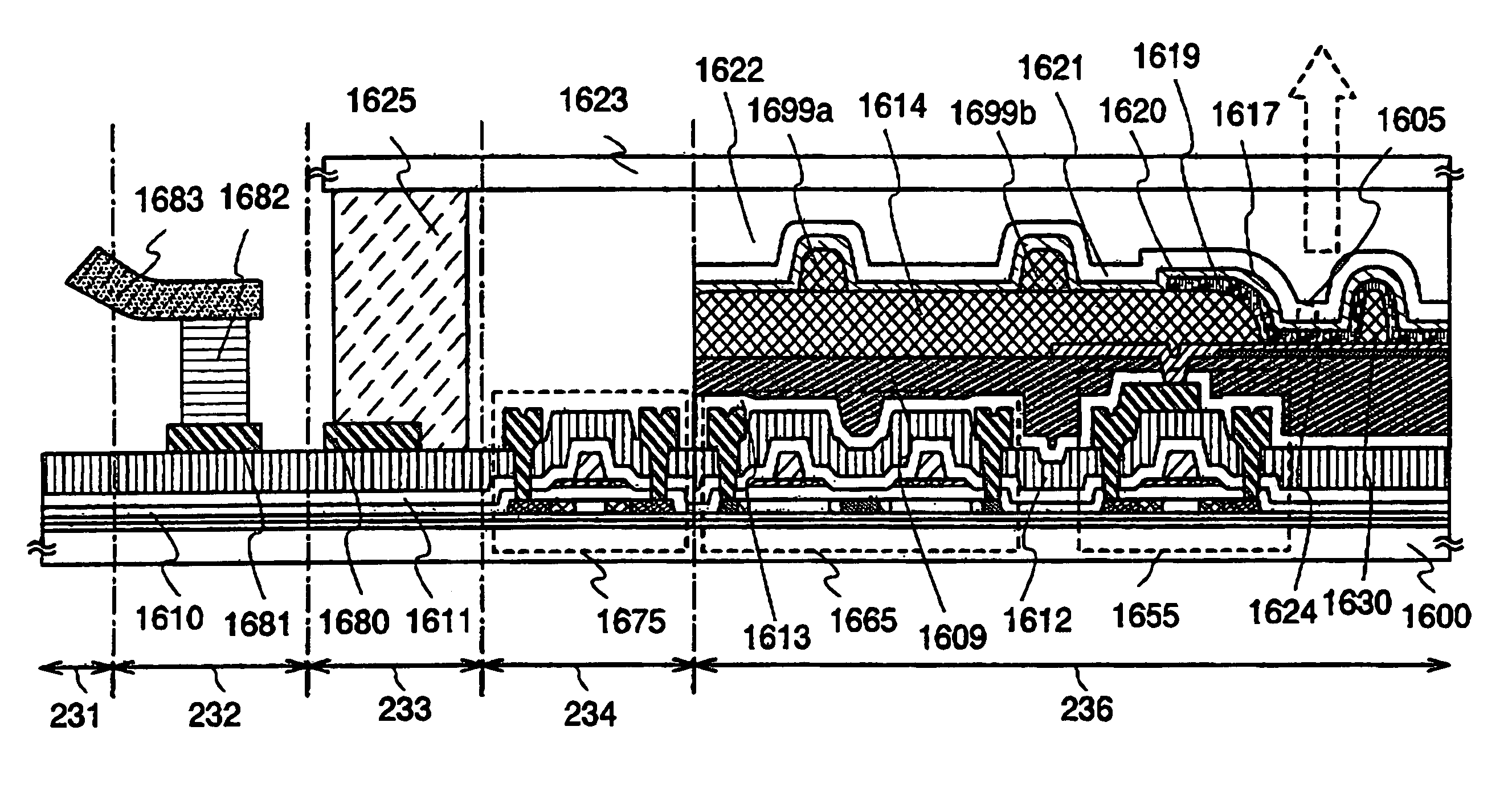
[0178]An embodiment mode of the invention is described with reference to FIGS. 7 to 9. This embodiment mode shows an example in which a second interlayer insulating layer is not formed in the display device manufactured in accordance with Embodiment Mode 1. Therefore, repetitive description on the same portion or a portion having a similar function is omitted.

[0179]As shown in Embodiment Mode 1, the thin film transistor 173, the thin film transistor 174, thin film transistor 175, the thin film transistor 176, and the conductive layer 177 are formed over the substrate 100, and the insulating film 168 and the insulating film 168 are formed. A source electrode layer or drain electrode layer connected to a source region or drain region of a semiconductor layer is formed over each thin film transistor. A first electrode layer 395 in contact with the source electrode layer or drain electrode layer 172b in the thin film transistor 176 formed in the pixel region 206 is formed (see FIG. 7(A)...

embodiment mode 3

[0185]An embodiment mode of the invention is described with reference to FIG. 10. This embodiment mode shows an example in which a gate electrode layer structure of a thin film transistor is different in the display device manufactured in accordance with Embodiment Mode 1. Therefore, repetitive description on the same portion or a portion having a similar function is omitted.

[0186]Each of FIGS. 10(A) to (C) is a display device in a manufacturing step, and corresponds to the display device of Embodiment Mode 1 shown in FIG. 4(B).

[0187]In FIG. 10(A), a thin film transistor 273 and a thin film transistor 274 are provided in a peripheral driver circuit region 214, a conductive layer 277 is provided in a connecting region, and a thin film transistor 275 and a thin film transistor 276 are provided in a pixel region 216. A gate electrode layer of the thin film transistor in FIG. 10(A) is formed of stacked layers of two conductive films and an upper layer of the gate electrode layer is patt...


PUM

PropertyMeasurementUnit
thicknessaaaaaaaaaa
thicknessaaaaaaaaaa
thicknessaaaaaaaaaa

Abstract

It is an object of the invention to provide a technique to manufacture a display device with high image quality and high reliability at low cost with high yield. The invention has spacers over a pixel electrode layer in a pixel region and over an insulating layer functioning as a partition which covers the periphery of the pixel electrode layer. When forming a light emitting material over a pixel electrode layer, a mask for selective formation is supported by the spacers, thereby preventing the mask from contacting the pixel electrode layer due to a twist and deflection thereof. Accordingly, such damage as a crack by the mask does not occur in the pixel electrode layer. Thus, the pixel electrode layer does not have a defect in shapes, thereby a display device which performs a high resolution display with high reliability can be manufactured.

Description

TECHNICAL FIELD[0001]The present invention relates to a display device, an electronic apparatus, and a method of fabricating the display device.BACKGROUND ART[0002]In order to perform a full color display by a display device provided with an electroluminescence (hereinafter also referred to as EL) element, a color light emitting element which emits color light is used. One of important factors for forming a color light emitting element is to form a light emitting material of each color in a fine pattern over an electrode.[0003]For the aforementioned purpose, generally used is a method for forming a fine pattern using a mask when forming a material using a vapor deposition method and the like.[0004]However, there is a problem in that a defect occurs due to a precision and a deflection of a mask used in vapor deposition which is caused by the fineness of a pixel region in accordance with higher resolution and the large size of a substrate in accordance with a larger area. A research a...

Claims


Application Information

Patent Timeline
Patent Type & Authority Patents(United States)
IPC IPC(8): H01J9/24
CPCH01L27/3246H01L27/153H01L51/56Y02E10/549Y02P70/50H10K59/122H10K50/8428H10K71/00H10K50/805H10K50/84H05B33/22H05B33/10H10K50/11H10K59/123H10K59/38H10K59/124H10K59/1213H10K71/164H10K71/166H10K77/111H10K59/1201H10K2102/311H01L27/1222H01L27/1277H01L27/1288H01L29/78675
Inventor YAMAZAKI, SHUNPEI
Owner SEMICON ENERGY LAB CO LTD
Why Eureka
Try Eureka