Nonvolatile semiconductor memory device and data erase/write method thereof

a non-volatile semiconductor and memory device technology, applied in semiconductor devices, digital storage, instruments, etc., can solve the problem that the direction of the voltage to be applied to the variable resistor element cannot be changed

Active Publication Date: 2010-06-22
KIOXIA CORP
View PDF6 Cites 169 Cited by
  • Summary
  • Abstract
  • Description
  • Claims
  • Application Information

AI Technical Summary

Problems solved by technology

Thus, there is a tendency that the direction of the voltage that is to be applied to the variable resistor element cannot be changed, and data erase (reset) cannot be executed in units of the series-connected memory cell section (memory cell string) (2).

Method used


Image

  • Nonvolatile semiconductor memory device and data erase/write method thereof
  • Nonvolatile semiconductor memory device and data erase/write method thereof
  • Nonvolatile semiconductor memory device and data erase/write method thereof

Examples


first embodiment

1. Entire Structure

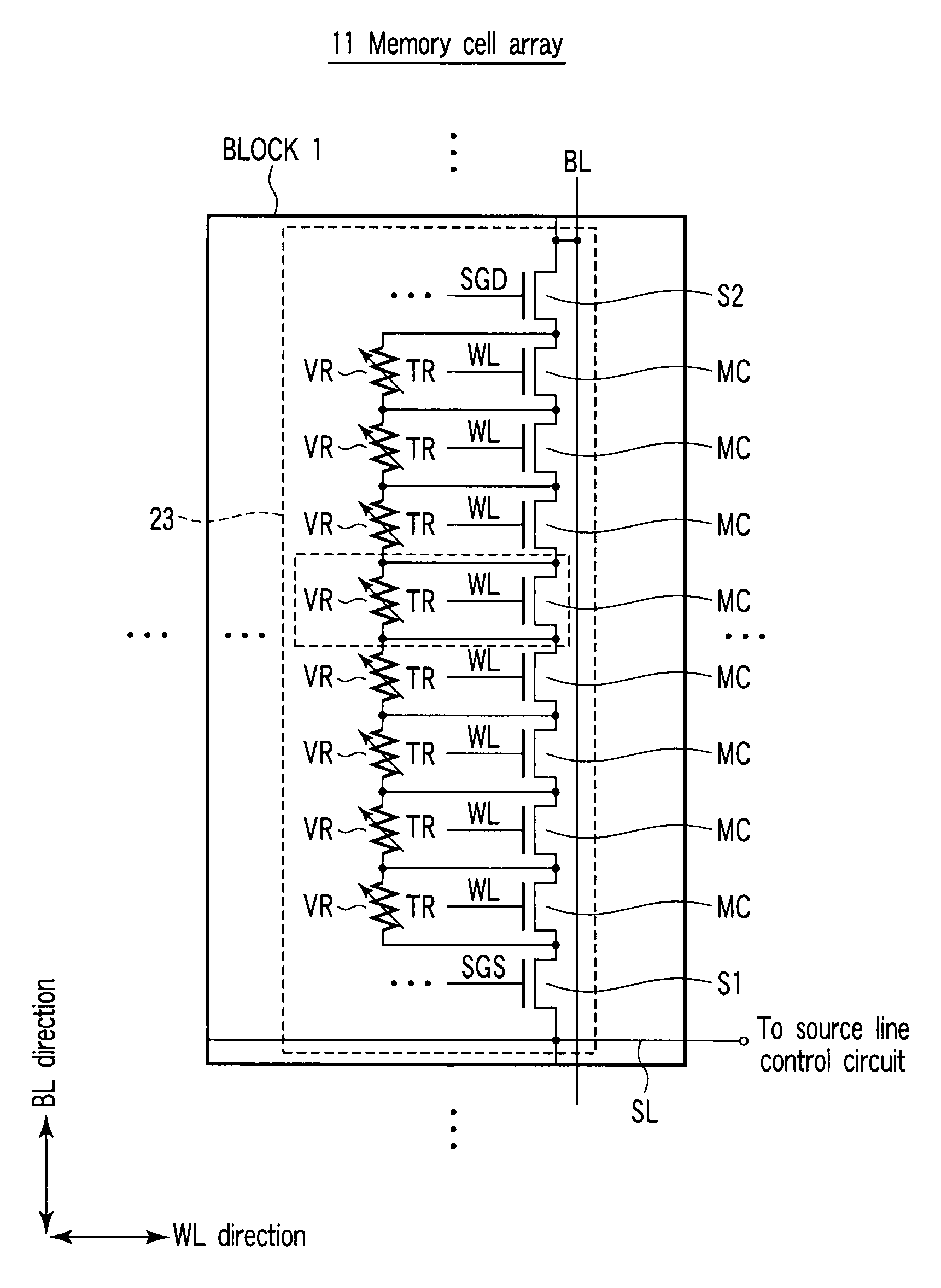
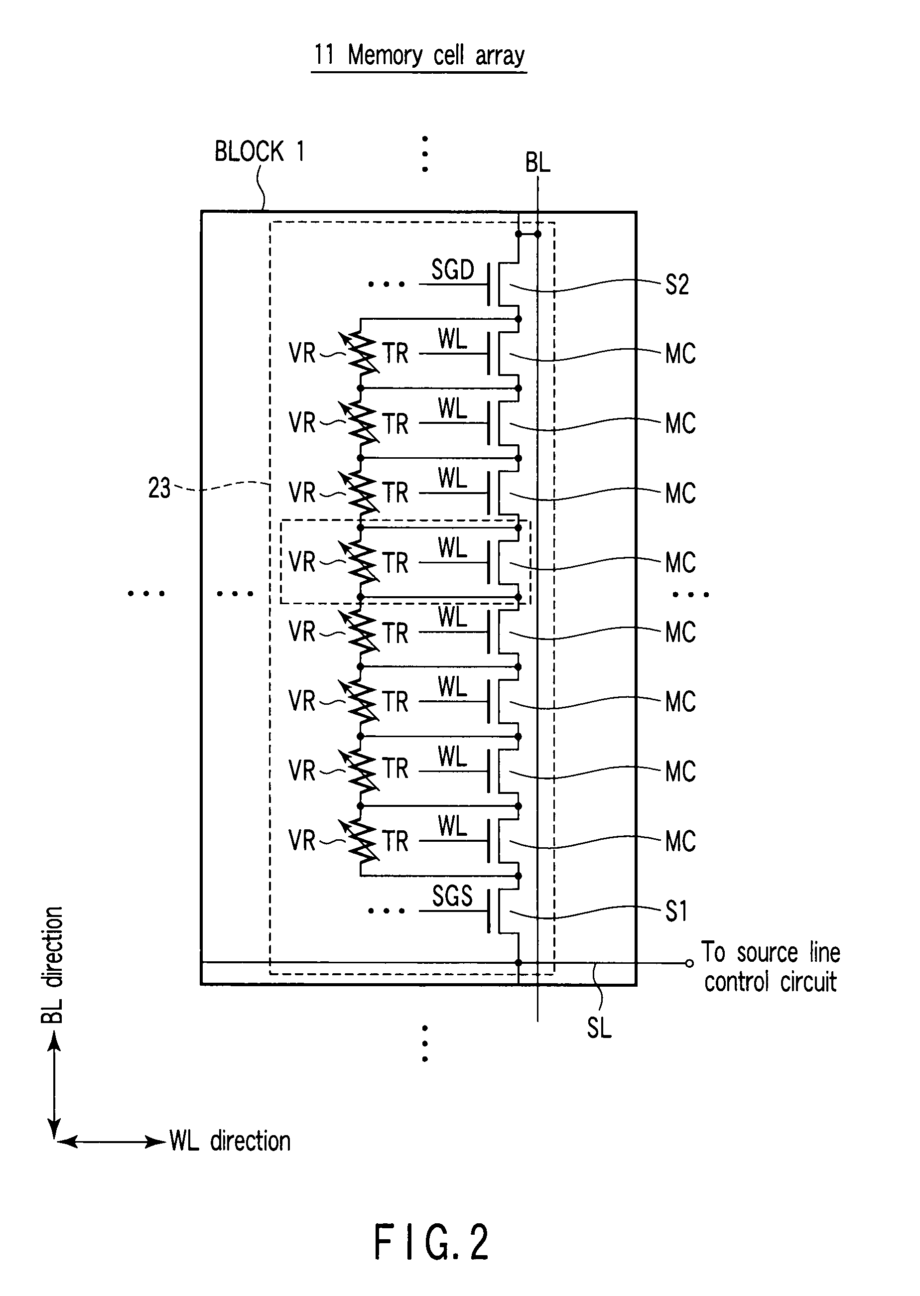
[0046]To begin with, referring to FIG. 3, a description is given of the entire structure of a nonvolatile semiconductor memory device according to a first embodiment of the present invention. FIG. 3 is a block diagram showing the nonvolatile semiconductor memory device according to this embodiment.

[0047]As shown in FIG. 3, the nonvolatile semiconductor memory device comprises a memory cell array 11, a bit line control circuit 12, a column decoder 13, a data input / output buffer 14, a data input / output terminal 15, a word line control circuit 16, a control signal & control voltage generating circuit 17, a control signal input terminal 18 and a source line control circuit 19.

[0048]The memory cell array 11 is composed of a plurality of blocks. The word line control circuit 16 for controlling word lines, the bit line control circuit 12 for controlling bit lines and the source line control circuit 19 for controlling the source line are connected to the memory cell array...

second embodiment

Another Example of the Structure of the Memory Cells

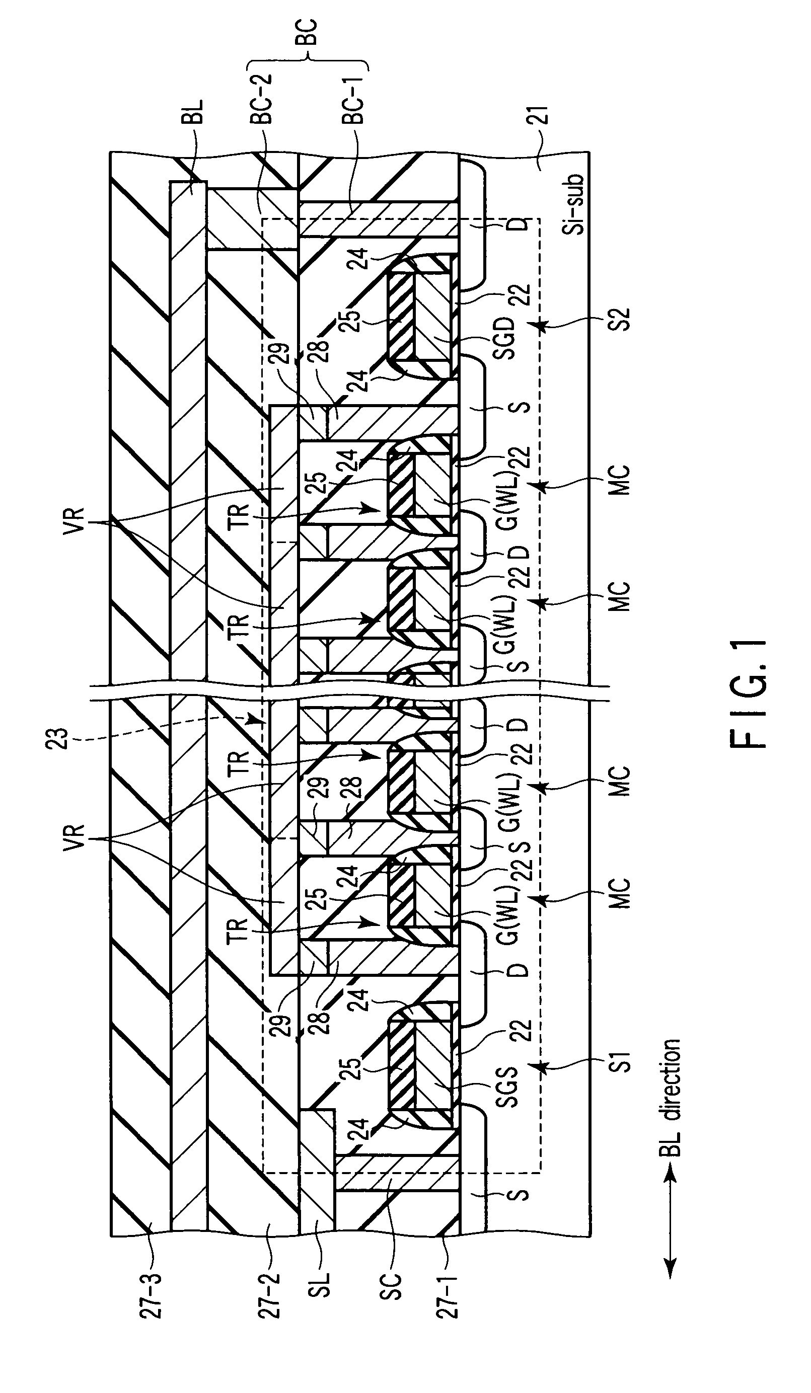
[0117]Next, the structure of a nonvolatile semiconductor memory device according to a second embodiment of the invention is described with reference to FIG. 15 and FIG. 16. This embodiment relates to another example of the structure of the memory cells. FIG. 15 is a plan view showing a nonvolatile semiconductor memory device according to this embodiment. FIG. 16 is a cross-sectional view taken along line XVI-XVI in FIG. 15. A detailed description of the parts common to those in the first embodiment is omitted here.

[0118]As shown in FIG. 16, the nonvolatile semiconductor memory device of the second embodiment differs from that of the first embodiment in that variable resistor elements VR1 to VR8 are buried in the interlayer insulator film 27-1. The depth of the trench in which the variable resistor element, VR1 to VR8, is buried is set to be shallower than the depth of the trench in which the electrode 29 is buried.

[0119]The operati...

third embodiment

An Example of the Structure of a Vertical-Type Nonvolatile Semiconductor Memory Device

[0132]Next, a nonvolatile semiconductor memory device according to a third embodiment of the present invention is described. The present embodiment relates to an example of the structure of a vertical-type nonvolatile semiconductor memory device. A detailed description of the parts common to those in the first embodiment is omitted here.

[0133]A structure example of the nonvolatile semiconductor memory device is described with reference to FIG. 19 and FIG. 20. FIG. 19 is a plan view showing the nonvolatile semiconductor memory device according to the third embodiment. FIG. 20 is a cross-sectional view taken along line XX-XX in FIG. 19.

[0134]As shown in FIG. 20, the nonvolatile semiconductor memory device according to the third embodiment is a vertical-type nonvolatile semiconductor memory device wherein a select transistor S1, memory cells MC1 to MC4 and a select transistor S2 are successively provi...


PUM


Abstract

A nonvolatile semiconductor memory device includes a memory cell array which includes a memory cell string including a plurality of memory cells each having a variable resistor element and a switching element having a current path with one end and the other end, between which the variable resistor element is connected, the plurality of memory cells having current paths thereof being connected in series, the memory cell array further including a first select element connected to one end of a current path of the memory cell string, and a second select element connected to the other end of the current path of the memory cell string, a bit line which is electrically connected to one end of a current path of the first select element, and a source line which is electrically connected to one end of a current path of the second select element.

Description

CROSS-REFERENCE TO RELATED APPLICATIONS[0001]This application is based upon and claims the benefit of priority from prior Japanese Patent Application No. 2007-087201, filed Mar. 29, 2007, the entire contents of which are incorporated herein by reference.BACKGROUND OF THE INVENTION[0002]1. Field of the Invention[0003]The present invention relates to a nonvolatile semiconductor memory device and a data erase / write method thereof, and is applied, for example, to a ReRAM (resistive memory) using a variable resistor element in which a resistance value varies depending on the direction of a voltage that is applied.[0004]2. Description of the Related Art[0005]In recent years, studies have been made on the application of, e.g. a ReRAM (resistive memory) using a variable resistor element in which a resistance value varies depending on the direction of a voltage that is applied. As disclosed in, for instance, Jpn. Pat. Appln. KOKAI Publication No. 2004-272975 and S.Q. Liu, N. J. Wu, A. Ignati...

Claims


Application Information

Patent Timeline
Patent Type & Authority Patents(United States)
IPC IPC(8): G11C11/00
CPCG11C13/0004G11C13/0007G11C13/003G11C2213/31G11C2213/32G11C2213/71G11C2213/75H01L27/101H01L27/105H10B63/34H10B63/84H10B63/30H10B63/80H10N70/823H10N70/231H10N70/20H10N70/826H10N70/8836H10N70/8833H10B99/00
Inventor WATANABE, TOSHIHARU
Owner KIOXIA CORP
Why Eureka
Try Eureka