
Circuit devices

a technology of circuit devices and circuits, applied in static indicating devices, instruments, electroluminescent light sources, etc., can solve the problems of increasing the number of fabrication processes required for transistors, and achieve the effect of wide design flexibility and reducing the number of fabrication processes required

Active Publication Date: 2010-08-03
INNOLUX CORP
View PDF2 Cites 0 Cited by
  • Summary
  • Abstract
  • Description
  • Claims
  • Application Information

AI Technical Summary

Benefits of technology

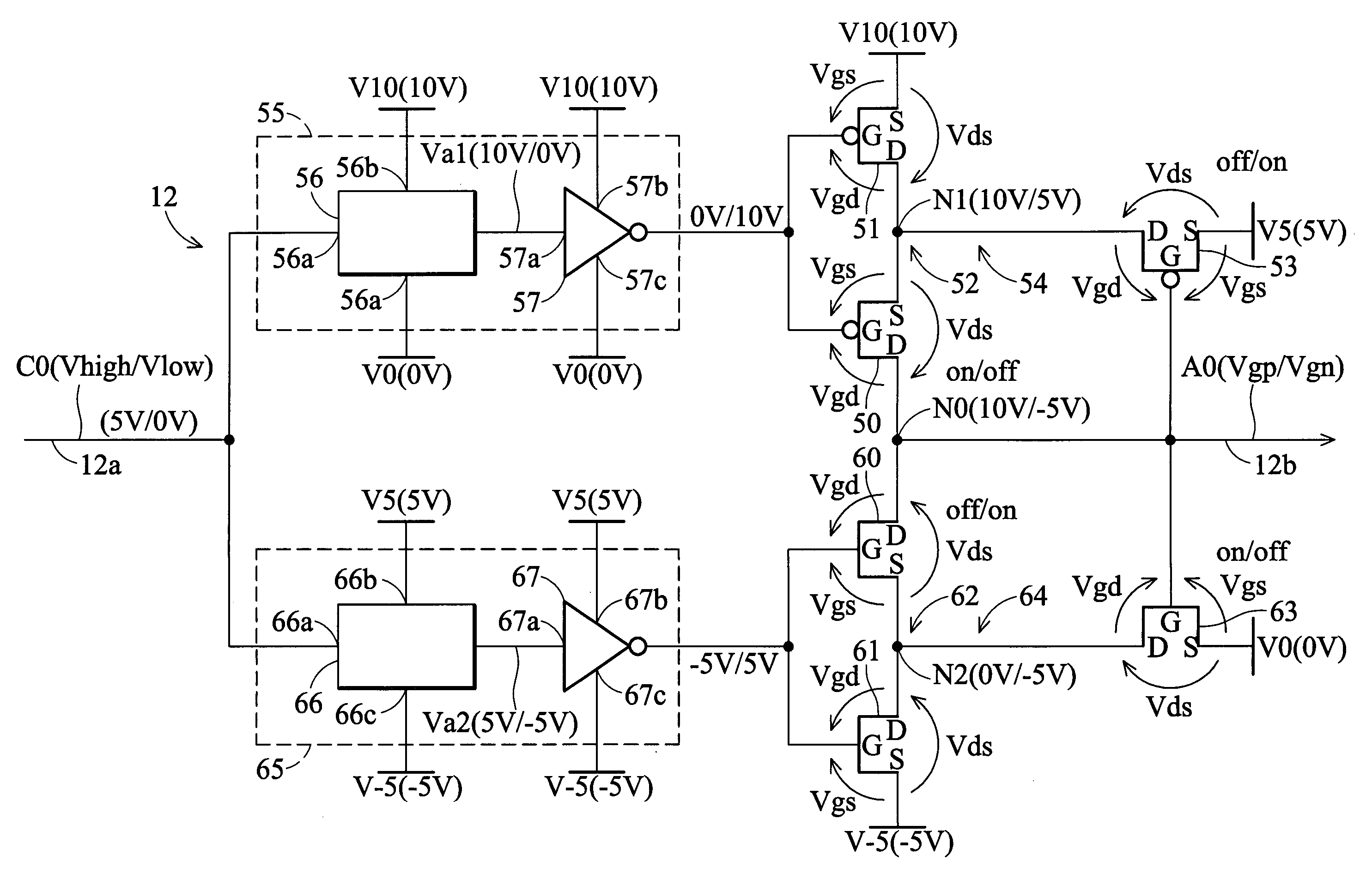
The invention provides a circuit device that requires fewer processes for fabricating transistors. The device has multiple routes for voltage application, which allows for separate control of different transistors. This reduces the risk of damage to transistors and allows for the use of more flexible switching devices. The device can use the same process for all switching devices, reducing the number of fabrication processes required. Overall, the invention improves the efficiency and flexibility of circuit devices.

Problems solved by technology

However, transistors of different gate insulating films cannot be formed by the same fabricating process, thus, required different processes for fabricating such transistors increase.

Method used


Image

  • Circuit devices
  • Circuit devices
  • Circuit devices

Examples


Embodiment Construction

[0027]The following description is of the best-contemplated mode of carrying out the invention. This description is made for the purpose of illustrating the general principles of the invention and should not be taken in a limiting sense. The scope of the invention is best determined by reference to the appended claims.

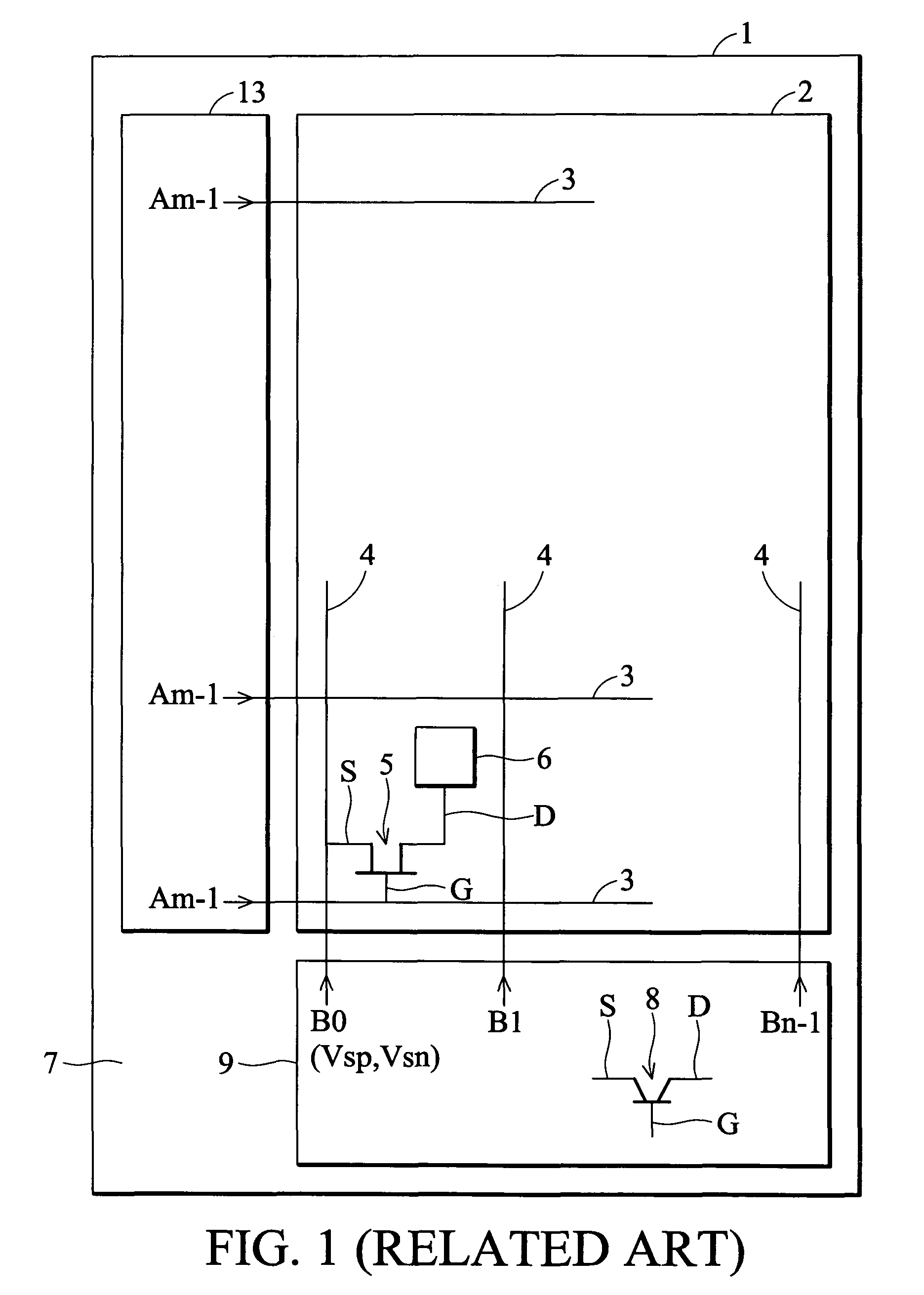
[0028]FIG. 1 is a block diagram of a circuit formed on glass substrate.

[0029]Display region 2 and non-display region 7 are disposed on a glass substrate 1. Gate driver 13 is formed in the non-display region 7, having a second circuit portion 12 (referring to FIGS. 3 and 5) as one of its features. First the whole circuit formed on the glass substrate 1 is described hereinafter, and then the second circuit portion 12 (referring to FIGS. 3 and 5) is described.

[0030]In display region 2 on the glass substrate 1, m gate lines 3 and n source lines 4 are formed, and TFT (thin film transistor) 5 is formed at intersection of gate line 3 and source line 4. Gate G of TFT 5 is coup...


PUM


Abstract

The invention provides a circuit device for reducing the number of fabrication processes. A circuit portion 12 provides power supply voltage V10 to a node N0 through a first route 52 and power supply voltage V−5 to the node N0 through a second route 62. The circuit device includes a TFT 50 disposed on the first route 52, a TFT 60 disposed on the first route 52 and coupled to the TFT 50, a TFT 60 disposed on the second route 62, a TFT 61 disposed on the second route 62 and coupled to the TFT 60, a third route 54 providing power supply voltage V5 between V10 and V−5 to between the TFT 50 and 51, and a fourth route 64 providing power supply voltage V0 between V10 and V−5 to between the TFT 60 and 61.

Description

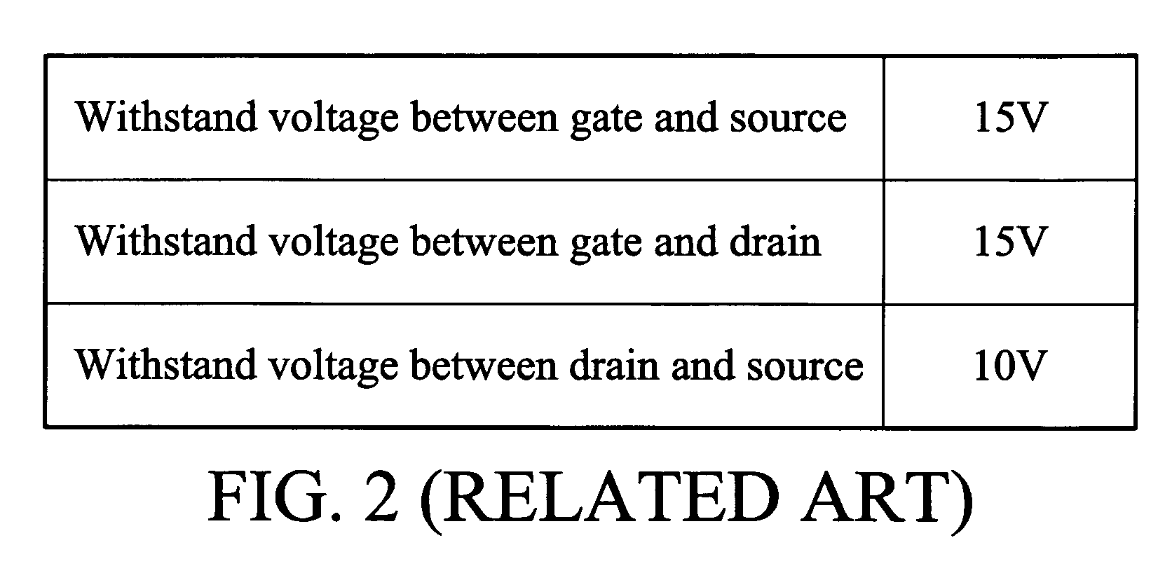
BACKGROUND OF THE INVENTION[0001]1. Field of the Invention[0002]The invention relates to a circuit device providing a first voltage to a node through a first route and a second voltage providing a second voltage to the node through a second route.[0003]2. Description of the Related Art[0004]Recent technologies used in formation of thin film transistors (TFTs) on glass substrate have developed with utilization of low temperature polysilicon. Such technologies are also applied in manufacture of display panels, wherein TFT array is formed on a display region of a glass substrate while gate driver and source driver are formed on a non-display region around the display region.[0005]Generally, when a gate driver receives a signal, it shifts voltage level of the received signal. Accordingly, the gate driver comprises transistors of different withstanding voltages.[0006]To form transistors of different withstanding voltages, thicknesses, for example, of gate insulating films of transistors ...

Claims


Application Information

Patent Timeline
Patent Type & Authority Patents(United States)
IPC IPC(8): G09G3/36H05B44/00
CPCG09G3/3677G09G5/10G09G2310/0275G09G2310/0289H01L27/12
Inventor HASHIMOTO, KAZUYUKI
Owner INNOLUX CORP
Learn More