Test operation of multi-port memory device

a multi-port memory device and test operation technology, applied in the field of semiconductor memory devices, can solve the problems of inability to test the multi-port memory device correctly, the current use of most dram test devices cannot support the high data process speed provided by the ports, and the increase in data transmission costs when data transmission is performed

Active Publication Date: 2010-08-10
SK HYNIX INC
View PDF22 Cites 66 Cited by
  • Summary
  • Abstract
  • Description
  • Claims
  • Application Information

AI Technical Summary

Problems solved by technology

However, because a large number of buses are included for the parallel I / O interface, a data transmission cost increases when the data transmission is performed between long distance.
However, most DRAM test devices currently used cannot support the high data process speed provided by the ports.
Further, when the ports operate erroneously, it is impossible to test the multi-port memory device correctly.

Method used


Image

  • Test operation of multi-port memory device
  • Test operation of multi-port memory device
  • Test operation of multi-port memory device

Examples


Embodiment Construction

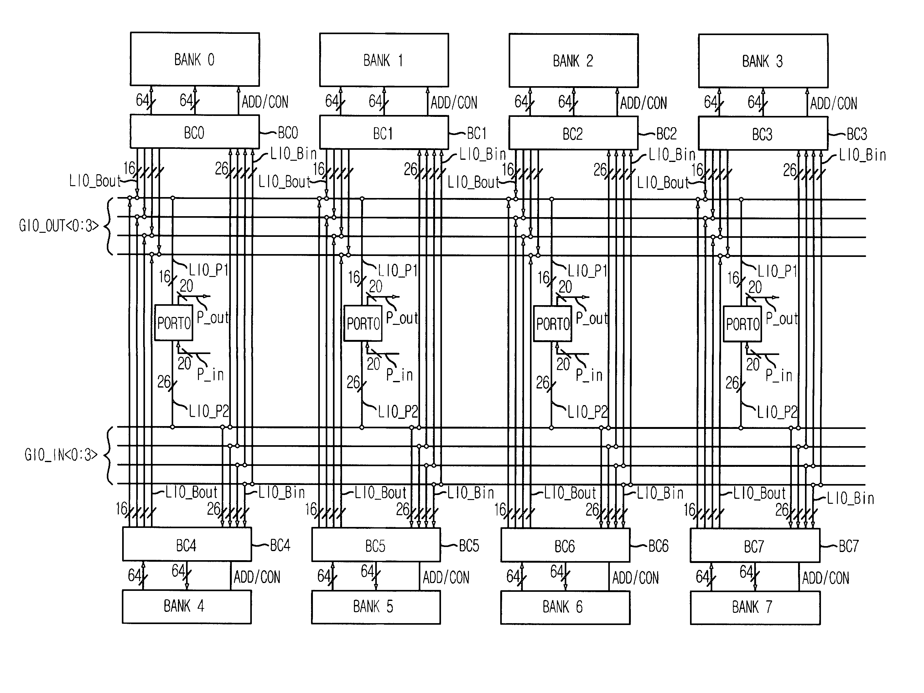
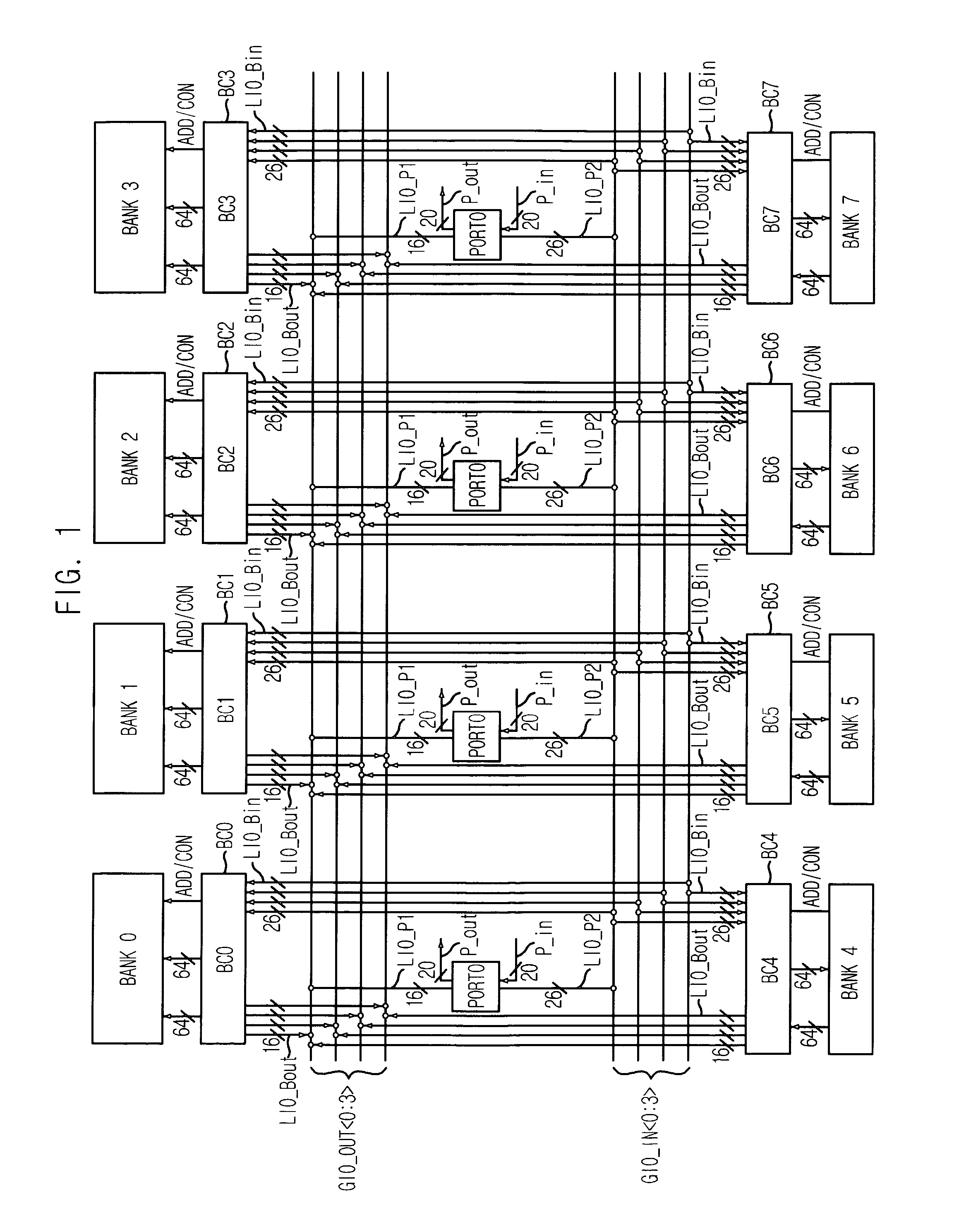
[0068]The multi-port memory device in accordance with the present invention performs the test operation by directly transmitting data between a test device and the banks without passing through the ports. Therefore, the test operation is effectively performed with the test devices whose data transmission speed is relatively slower than that of the ports. Further, the test reliability is improved because the test operation is not affected by port error. The present invention can be widely employed with multi-port memory devices for performing serial data transmission between external devices and the ports and performing parallel data transmission between the ports and the banks.

[0069]FIG. 9 is a block diagram of a multi-port memory device in accordance with an embodiment of the present invention.

[0070]For convenience of explanation, a multi-port memory device having four ports and eight banks is illustrated. Particularly, it is assumed that the multi-port memory device has a 16-bit d...


PUM


Abstract

A multi-port memory device includes a plurality ports, a plurality of banks, a plurality of global data buses, first and second I / O controllers, and a test input / output (I / O) controller. The ports perform a serial I / O data transmission. The banks perform a parallel I / O data transmission with the ports. The global data buses are employed for transmitting data between the ports and the banks. The first I / O controller controls a serial data transmission between the ports and external devices. The second I / O controller controls a parallel data transmission between the ports and the global buses. The test I / O controller generates test commands based on a test command / address (C / A) inputted from the external devices and transmits a test I / O data with the global data bus during a test operation mode.

Description

CROSS-REFERENCE TO RELATED APPLICATION[0001]The present invention claims priority of Korean patent application number 10-2006-0033750, filed on Apr. 13, 2006, which is incorporated by reference in its entirety.BACKGROUND OF THE INVENTION[0002]The present invention relates to a semiconductor memory device, and more particularly to a semiconductor memory device including a plurality of ports for transmitting information with external devices.[0003]Most memory devices such as a random access memory (RAM) include only one port for transmitting data with external chipsets. The port is constituted with a plurality of input / output (I / O) pins. The memory device including single port employs a parallel I / O interface for concurrently transmitting multi-bit data through a plurality of data lines connected to the plurality of I / O pins respectively. The I / O interface uses a data transmission scheme for transmitting data via data lines, each of which is connected between two devices. The data lin...

Claims


Application Information

Patent Timeline
Patent Type & Authority Patents(United States)
IPC IPC(8): G11C7/00
CPCG11C7/1012G11C7/1075G11C29/1201G11C29/14G11C29/48G11C2207/107G11C7/10
Inventor DO, CHANG-HOCHUNG, JIN-IL
Owner SK HYNIX INC
Why Eureka
Try Eureka